Stacked package structure of image sensor

a technology of image sensor and package structure, which is applied in the direction of semiconductor devices, semiconductor/solid-state device details, electrical devices, etc., can solve the problems of increasing manufacturing costs, light, thin, etc., and achieves the effect of reducing the number of package elements and lowering the cost of the packag

Inactive Publication Date: 2003-09-30
KINGPAK TECH INC
View PDF4 Cites 41 Cited by
  • Summary
  • Abstract
  • Description
  • Claims
  • Application Information

AI Technical Summary

Benefits of technology

It is therefore an object of the present invention to provide a stacked package structure of an image sensor for reducing the number of the package elements and lowering the package costs.
It is therefore another object of the present invention to provide a stacked package structure of an image sensor for simplifying and facilitating the manufacturing processes.
It is therefor still object of the present invention to provide a stacked package structure of an image sensor for lowering the area of the image sensor.
It is therefor yet object of the present invention to provide a stacked package structure of an image sensor for lowering the package costs and testing costs of the image sensing products.

Problems solved by technology

Thereafter, the image sensor is electrically connected to the signal processing units by a plurality of wirings, respectively, therefore, in order to individually package each of the signal processing units and the image sensor, a plurality of substrates and package bodied have to be used, thereby increasing the manufacturing costs.
Furthermore, the required area of the printed circuit board should be large when mounting each of the processing units onto the printed circuit board, so the products cannot be made small, thin, and light.

Method used


Image

  • Stacked package structure of image sensor
  • Stacked package structure of image sensor
  • Stacked package structure of image sensor

Examples


Embodiment Construction

The embodiment of the present invention will now be described reference to the drawings.

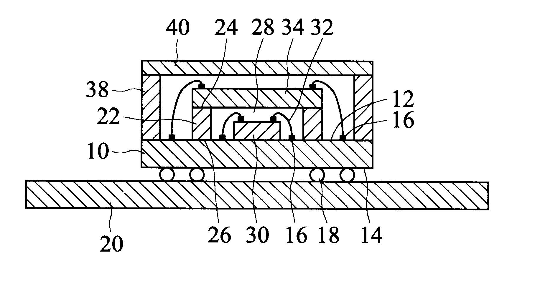
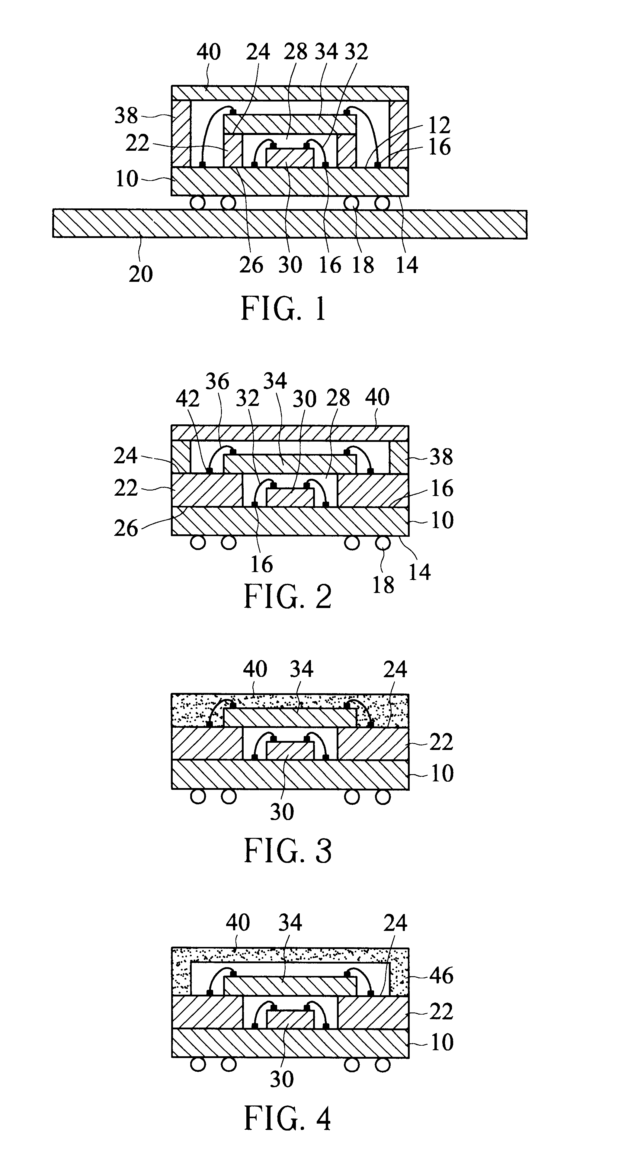
As shown in FIG. 1, the stacked package structure of an image sensor of the present invention includes a first substrate 10, a second substrate 22, an integrated circuit 30, an image sensing chip 34, a projecting structure 38 and a transparent layer 40.

The first substrate 10 has a first surface 12 and a second surface 14 opposite to the first surface 12. The first surface 12 of the first substrate 10 is formed with signal input terminals 16. The second surface 14 of the first substrate 10 is formed with signal output terminals 18, which may be metallic balls arranged in the form of ball grid array, for transmitting signals from the first substrate 10 to the printed circuit board 20.

The second substrate 22 has an upper surface 24 and a lower surface 26 opposite to the upper surface 24. The lower surface 26 of the second substrate 22 is adhered to the first surface 12 of the first substrate 10, so ...


PUM


Abstract

A stacked package structure of an image sensor for electrically connecting to a printed circuit board includes a first substrate, a second substrate, an integrated circuit, an image sensing chip, and a transparent layer. The second substrate is mounted on the first substrate so as to a cavity formed between the first substrate and second substrate. The integrated circuit is located within the cavity and electrically connected the first substrate. The image-sensing chip is arranged on the second substrate. The transparent layer covers over the image sensing chip, wherein the image sensing chip receives image signals via the transparent layer and transforms the image signals into electrical signals transmitted to the first substrate. Thus, the image sensing chip of the image sensing product and the integrated circuit can be integrally package.

Description

1. Field of the InventionThe present invention relates to a stacked package structure of an image sensor, in particular, to a structure in which integrated circuit and image sensing chip, both having different function, are packaged into a package body so as to reduce the number of the package substrates and to integrally package the integrated circuited and image sensing chip both having different functions.2. Description of the ArtA general sensor is used for sensing signals, which may be optical or audio signals. The sensor of the present invention is used for receiving images and transforming the image signals into electrical signal to be transmitted to a printed circuit board.A general sensor is used for receiving image signals and converting the image signals into electrical signals that are transmitted to a printed circuit board. The image sensor is then electrically connected to other integrated circuit to have any required functions. For example, the image sensor may be ele...

Claims


Application Information

Patent Timeline
Patent Type & Authority Patents(United States)
IPC IPC(8): H01L23/02
CPCH01L27/14618H01L2224/48091H01L2224/48227H01L2924/15311H01L2924/00014
Inventor TU, HSIU WENCHEN, WEN CHUANHO, MON NANCHEN, LI HUANYEH, NAI HUAHUANG, YEN CHENGCHIU, YUNG SHENGWU, JICHENLIU, JOELEE, WU HSIANG
Owner KINGPAK TECH INC
Why Eureka
Try Eureka