E-field-modulated bistable molecular mechanical device

a mechanical device and field-modulated technology, applied in non-linear optics, instruments, nanoinformatics, etc., can solve the problems of inability to switch, slow switching times of molecules, and expenditure of significant amount of energy to toggle switches, and achieve maximum interaction strength.

Inactive Publication Date: 2004-06-15
SAMSUNG ELECTRONICS CO LTD
View PDF1 Cites 12 Cited by
  • Summary
  • Abstract
  • Description
  • Claims
  • Application Information

AI Technical Summary

Benefits of technology

The present invention introduces a new type of switching mechanism, namely, an electric field induced rotation of a rotatable middle section (rotor) of a molecule. Thus, the molecule is neither oxidized nor reduced in the toggling of the switch, which avoids the necessity of breaking chemical bonds and potentially initiating a nonreversible reaction. Also, the part of the molecule that moves is quite small, so the switching time should be very fast. Also, the molecules are much simpler and thus easier and cheaper to make than the rotaxanes and related compounds.
The present invention disclosure is an improvement over the foregoing applications and patent in that it is directed to a class of molecules that provides switching from one state to a different state, characterized by a change in the electrical conductivity. The three-branch or "Y" configuration of the molecular switches creates an optical alignment between the dipole movement of the rotor and the direction of the electric field between the electrodes. Further, the "Y" orientation allows the maximum interaction strength between the rotor dipole and the switching electric field.

Problems solved by technology

The primary problem with the rotaxane was that it is an irreversible switch.
This requires the expenditure of a significant amount of energy to toggle the switch.
In addition, the large and complex nature of rotaxanes and related compounds potentially makes the switching times of the molecules slow.
The primary problems with the catenanes are small ON-to-OFF ratio and a slow switching time.

Method used


Image

  • E-field-modulated bistable molecular mechanical device
  • E-field-modulated bistable molecular mechanical device
  • E-field-modulated bistable molecular mechanical device

Examples


second embodiment

Since each colorant molecule in colorant layer 301 is transparent outside of the colorant absorption band, then multiple colorant layers may be superimposed and separately addressed to produce higher resolution color displays than currently available. FIG. 4 is a schematic illustration of this A high resolution, full color, matrix addressable, display screen 400 comprises alternating layers of transparent electrodes--row electrodes 401, 403 and column electrodes 402 and 404--and a plurality of colorant layers 405, 407, 409, each having a different color molecule array. Since each pixel in each colorant layer may be colored or transparent, the color of a given pixel may be made from any one or a combination of the color layers (e.g., cyan, magenta, yellow, black) at the full address resolution of the display. When all colorant layers 405, 407, 409 for a pixel are made transparent, then the pixel shows the background substrate 303 (e.g., white). Such a display offers the benefit of t...

third embodiment

More specifically, the third embodiment as shown in FIG. 5 comprises a display screen 502, a scanned electrode array 504, and array translation mechanism 501 to accurately move the electrode array across the surface of the screen. The display screen 502 again comprises a background substrate 303, a transparent view-through layer 305, and at least one bi-stable molecule colorant layer 301. The colorant layer 301 may include a homogeneous monochrome colorant (e.g., black) or color mosaic, as described herein above. The scanned electrode array 504 comprises a linear array or equivalent staggered array of electrodes in contact or near contact with the background substrate 303. A staggered array of electrodes may be used, for example, to minimize field crosstalk between otherwise adjacent electrodes and to increase display resolution.

In operation, each electrode is sized, positioned, and electrically addressed to provide an appropriate electric field, represented by the arrow labeled "E"...

examples 1a and 1b

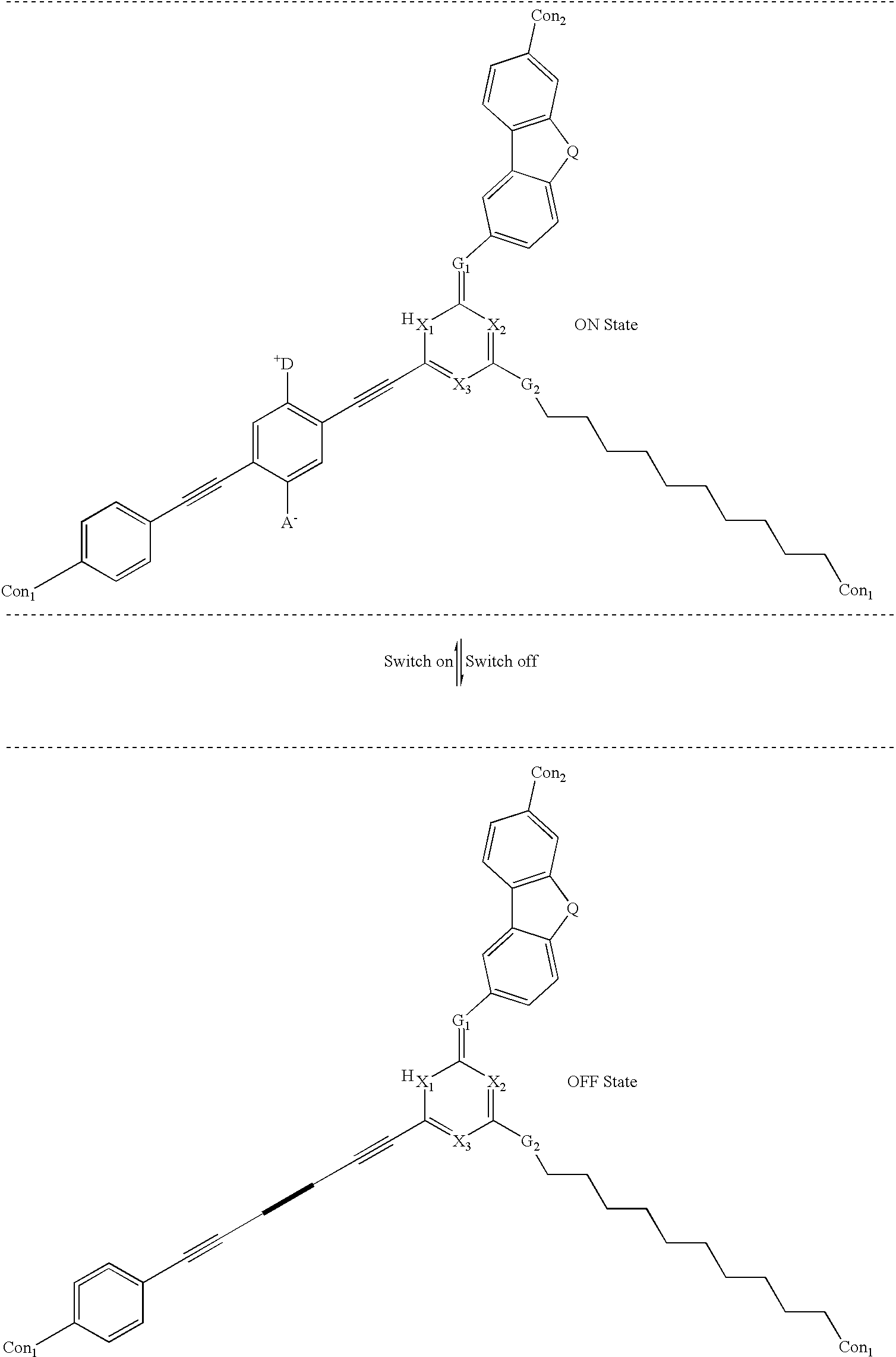
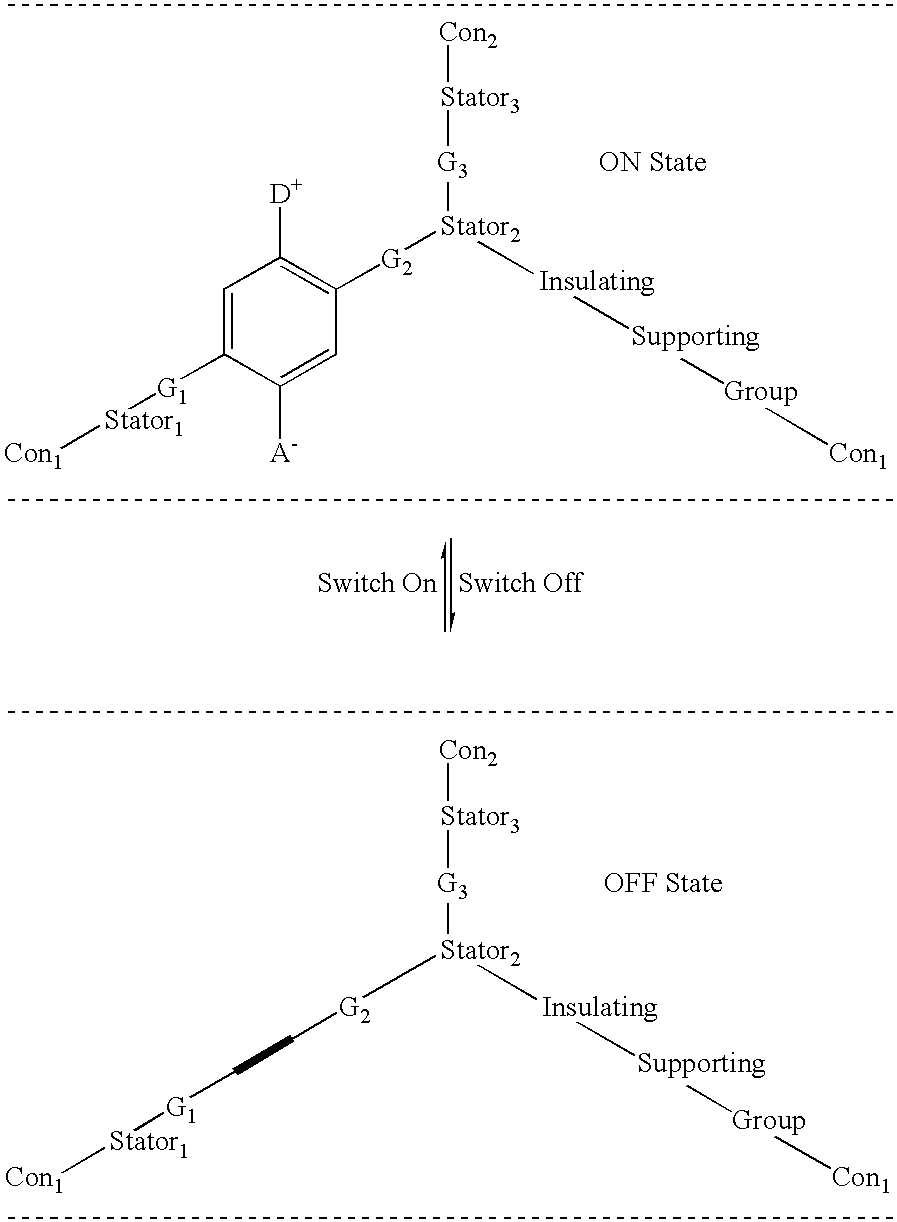
below show two different orientations for switching the molecules. In those examples, the rotation axis of the rotor is designed to be in 30 to 70 degree angle to the orientation axis of the molecules. The "Y" configuration of the molecule is chosen in order to orient the dipole movement of the rotor along the electric field direction between the electrodes in the "ON" state. This maximizes the strength of the interaction between the dipole movement and the electric field. This design allows different geometries of molecular films and electrodes to be used, depending on the desired results.

Turning first to Example 1a, this depicts a first generic molecular example for the present invention. Example 1b, which follows, depicts a specific molecular system. ##STR1##


PUM

PropertyMeasurementUnit
angleaaaaaaaaaa
sizeaaaaaaaaaa
heightsaaaaaaaaaa

Abstract

A molecular system is provided for nanometer-scale reversible electronic and optical switches, specifically, electric field-activated molecular switches that have an electric field induced band gap change that occurs via a molecular conformation change or a tautomerization. Changing of extended conjugation via chemical bonding change to change the band gap is accomplished by providing the molecular system with one rotating portion (rotor) and two or more stationary portions (stators), between which the rotor is attached. The molecular system of the present invention has three branches (first, second, and third branches) with one end of each branch connected to a junction unit to form a "Y" configuration. The first and second branches are on one side of the junction unit and the third branch is on the opposite side of the junction unit. The first branch contains a first stator unit in its backbone, the junction unit comprises a second stator unit, and the first branch further contains a rotor unit in its backbone between the first stator unit and the second stator unit. The second branch includes an insulating supporting group in its backbone for providing a length of the second branch substantially equal to that of the first branch, wherein the rotor unit rotates between two states as a function of an externally-applied field.

Description

The present application is directed to a specific molecular system that involves at least one rotatable segment (rotor or rotors) that has a large dipole moment and that links with at least two other portions of the molecule that are immobilized (stators). The molecular system disclosed herein provides switching from one state to a different state, characterized by a change in the electronic properties and / or the optical properties of the molecules.The present invention relates generally to electronic and optical devices whose functional length scales are measured in nanometers, and, more particularly, to classes of molecules that provide electronic and optical switching. Electronic and optical devices both of micrometer and nanometer scale may be constructed in accordance with the teachings herein.The area of molecular electronics is in its infancy. To date, there have been two convincing demonstrations of molecules as electronic switches published in the technical literature; see,...

Claims


Application Information

Patent Timeline
Patent Type & Authority Patents(United States)
IPC IPC(8): G02F1/01G02B26/02G02F1/15G02F1/17G11C13/02H01L27/28H01L51/00
CPCH01L51/0071H01L51/0595B82Y10/00G02B26/026G02F1/15G02F1/174G11C13/0014G11C13/02G11C2213/71G11C2213/77G11C2213/81H01L27/285G11C13/04G11C23/00G11C2213/14H10K19/202H10K85/657H10K10/701
Inventor ZHANG, XIAO-ANZHOU, ZHANG-LINWILLIAMS, R. STANLEYVINCENT, KENT D.
Owner SAMSUNG ELECTRONICS CO LTD
Why Eureka
Try Eureka