Method and apparatus for resolving conflicts in a substrate processing system

a technology of a processing system and a substrate, applied in the field of microelectronic fabrication, can solve problems such as reducing expected throughput, inconsistent process results from substrate to substrate, and degrading not only throughput but also the process

Inactive Publication Date: 2004-07-27
ASML HLDG NV
View PDF38 Cites 31 Cited by
  • Summary
  • Abstract
  • Description
  • Claims
  • Application Information

AI Technical Summary

Benefits of technology

Another primary goal of the invention is to enable flexible synchronization of the fabrication system, ensuring that substrate processing and transportation occur at regular, predictable intervals without diminishing the throughput.
With respect to yet another aspect of the invention, a clustered wafer track and lithography system is provided. The benefits of the invention as described herein extend beyond a wafer track alone and are applicable to a combined wafer track and stepper apparatus. The synchronization and optimization of processing substrates in accordance with the invention efficiently achieves high and reliable throughput that can be measured and observed on a systemwide level.

Problems solved by technology

1) The delivery and removal of the substrate to and from the process modules, as well as the transportation of the wafer between modules, must be accomplished in a timely manner. This timely delivery and removal of substrate is achieved when the flow of substrate is maintained in a periodic and synchronized manner. If periodicity and synchronization are not maintained, the process results will be inconsistent from substrate to substrate, and the expected throughput may be reduced.
2) It is desirable to transport the substrate in similar process flow paths to avoid inconsistency in process results due to variations in the process history of the substrates.
3) It is imperative to ensure that the articles of manufacture do not spend any pre-process or post-process time idling in modules where critical processes are performed. The addition of pre-process or post-process time in these modules degrades not only the throughput but also the process results. For example, in an IC fabrication system, if a substrate is not immediately transferred from the spin coat module to a bake module to thermally cure a photo-resist film layer, the resulting film thickness will be unpredictable. If it is impossible to totally eliminate pre-process and / or post-process times, they should be rendered as brief as possible, and any variations in these times cannot be allowed.
The inability to meet any or all of the above conditions come from the failure to resolve transport conflicts.
Conflicts are situations wherein separate modules demand a robot within a time span insufficient for the robot to service these modules
However, the size limitations and geometrical constraints of a track system limit the possibility of resolving the above difficulties by adding additional process modules or transportation resources.
Dedicated transfer arms complicate the tool and increase its cost, constrain the position of the modules, and cannot be used everywhere in the tool.
As a result, the tasks of managing the substrate flow in the track system while maintaining both high throughput and quality and resolving all transport conflicts become unmanageable.
However, to achieve high throughputs, the scheduler may generate undesirable, unpredictable and variable pre-process and post-process times in critical modules, and the substrates may also be forced to follow different flow paths to complete their process cycle.
Heretofore, the semiconductor processing requirements of conflict resolution, synchronization, quality, and path consistency referred to above have not been fully met.

Method used


Image

  • Method and apparatus for resolving conflicts in a substrate processing system
  • Method and apparatus for resolving conflicts in a substrate processing system
  • Method and apparatus for resolving conflicts in a substrate processing system

Examples


Embodiment Construction

The invention and the various features and advantageous details thereof are explained more fully with reference to the non-limiting embodiments that are illustrated in the accompanying drawings and detailed in the following description of preferred embodiments. Descriptions of well-known components and processing techniques are omitted so as not to unnecessarily obscure the invention in detail.

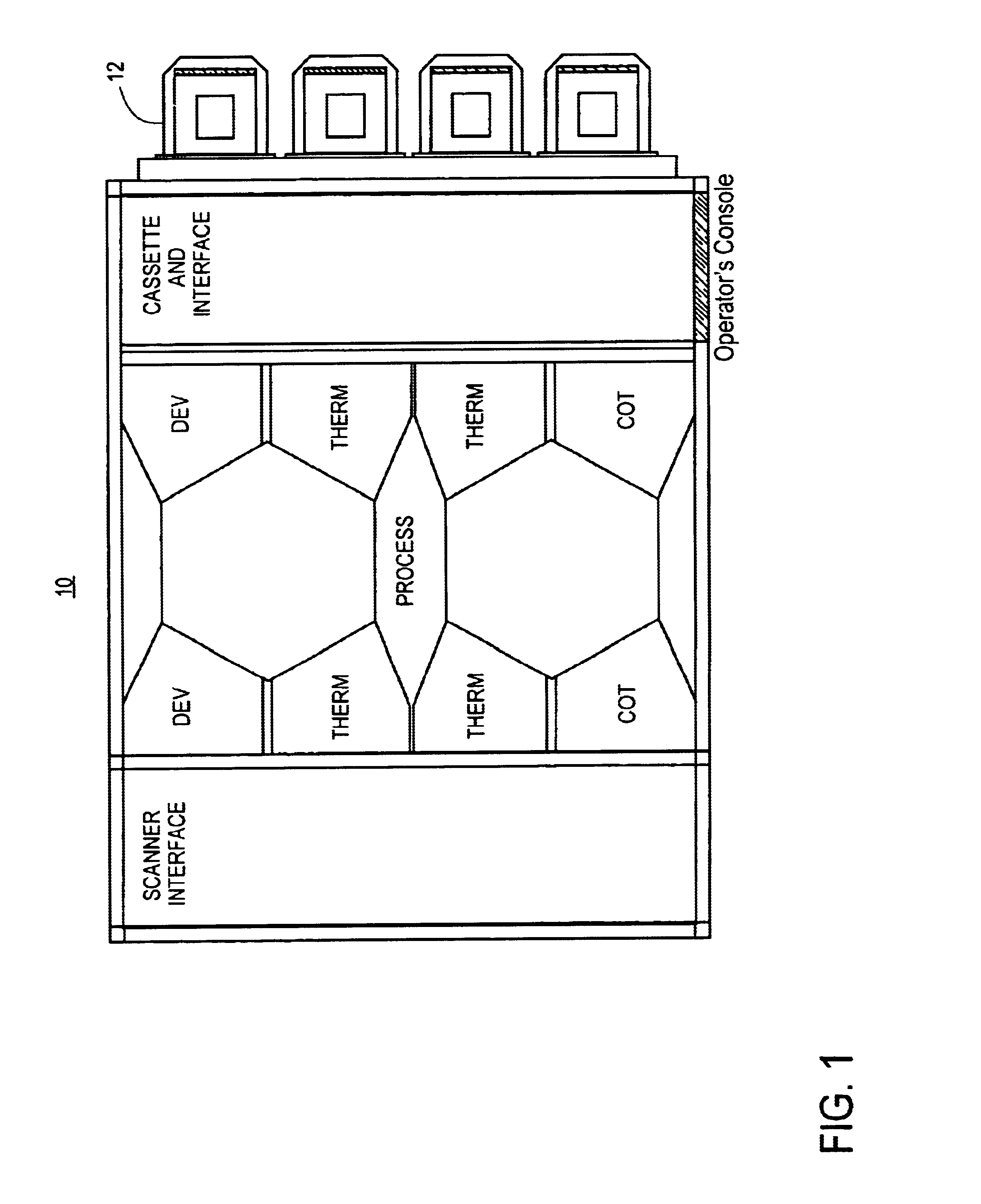
The invention herein may be applied to semiconductor processing equipment such as the wafer track system generally described in FIG. 1. The wafer track system 10 may include basically three sections: a cassette end interface section, a scanner interface section, and a process section. The cassette end interface section includes apparatus to transfer wafers from cassettes in which they are stored to the track system 10 and, conversely, from the track system back to cassettes following processing. The scanner interface section may be considered another transition area that accommodates equipment...


PUM


Abstract

A wafer track and lithography cluster tool for performing a series of processes with a scheduler which synchronizes all events in a substrate processing system. Events in the cluster tool are scheduled to occur at regular, periodic intervals, thereby improving throughput and quality. The scheduler also eliminates conflicts for transportation resources between modules in the cluster tool. Wafers are loaded into the cluster tool at a regular interval, referred to as a sending period. All events in the system are synchronized with the sending period, and all event timings are normalized in terms of the sending period. The conflicts are resolved by selectively adding delays in modules which can tolerate them without degrading throughput or performance in the system; modules that cannot tolerate delays are exempted. The periodicity of the scheduled cluster tool enables the identification of wafers in the cluster tool. The identification of the order in which a wafer was loaded also identifies a module path followed by the wafer.

Description

1. Field of the InventionThe invention relates generally to the field of microelectronic fabrication. More particularly, the invention relates to a technique of optimizing the throughput, reliability, and quality of microelectronic fabrication by synchronizing the individual processing and transportation mechanisms within a fabrication system.2. Discussion of the Related ArtIn the process of manufacturing a semiconductor device such as an integrated circuit, numerous steps of micro-fabrication are performed to form a device. These steps are performed serially on the individual items of manufacture in individual modules; the items of manufacture are transferred between modules by transport mechanisms such as robots. In order to achieve desirable throughput, reliability, and fabrication quality, several conditions must be met:1) The delivery and removal of the substrate to and from the process modules, as well as the transportation of the wafer between modules, must be accomplished in...

Claims


Application Information

Patent Timeline
Patent Type & Authority Patents(United States)
IPC IPC(8): G06F7/00G06F19/00
CPCG05B19/41865G05B2219/32048G05B2219/32065G05B2219/45031Y02P90/02
Inventor OH, HILARIO
Owner ASML HLDG NV
Why Eureka
Try Eureka