Solid state image pickup device and method of producing solid state image pickup device

a pickup device and solid state technology, applied in the direction of television systems, transistors, radio control devices, etc., can solve the problems of wiring not being located, sensitivity lowered, characteristics lowered,

Inactive Publication Date: 2004-11-23
SONY CORP
View PDF6 Cites 124 Cited by
  • Summary
  • Abstract
  • Description
  • Claims
  • Application Information

AI Technical Summary

Problems solved by technology

(1) Sensitivity is lowered as much as the amount of the light repelled by the wirings.
(2) A part of the light repelled by the wirings enters into the photodiode of the adjacent pixel, resulting in mixture of colors.
(3) Since the layout of the wirings is restricted, characteristics are lowered by the limitations such that the wirings cannot be located on the upper side of the photodiode, or thick wirings cannot be utilized.
(4) Miniaturization is difficult to achieve for the same reason as (3) above.
(5) Since skew incidence of light occurs and the proportion of the light repelled is higher at the pixels in a peripheral area, dark shading occurs more heavily in the peripheral area.
(6) When it is intended to produce the CMOS image sensor by an advanced CMOS process in which the number of the wiring layers is increased further, the distance from the micro-lens to the photodiode is enlarged, and the above difficulties are further increased.
(7) Due to (6) above, the typical advanced CMOS processing techniques cannot be used, correction of the layout of the circuits registered in the library is needed, or the number of the wiring layers is limited and therefore the area is enlarged, so that the cost is raised. Besides, the pixel area per pixel is also increased.
Therefore, the number of steps is increased, and the process becomes complicated.
In addition, defects in the photodiode arise from the steps, also.
Therefore, in the related-art method in which the light is passed to the light-receiving surface through the wiring layers, it has come to be impossible to efficiently condense the light onto the light-receiving surface of the pixel, and the problems of (1) to (7) above have come to be conspicuous.
However, the image pickup device with such a structure has the problem the sensitivity for blue color for which absorptivity is high is lowered.
From the above circumstances, the back-illuminated type CCD type image pickup device has almost not been put to practical use, and such a back-illuminated type CCD image pickup device in which color filters and micro-lenses are in an on-chip form are not typically utilized.
In addition, the structure in which a number of layers of metallic wirings extend in crossing directions is absent in the case of the CCD type image pickup device.
Therefore, in the case of producing the back-illuminated type CMOS image sensor, there is the problem that the registration mark formed at the time of producing the aluminum wiring layer cannot be used as it is as in a related art.

Method used


Image

  • Solid state image pickup device and method of producing solid state image pickup device
  • Solid state image pickup device and method of producing solid state image pickup device
  • Solid state image pickup device and method of producing solid state image pickup device

Examples


Embodiment Construction

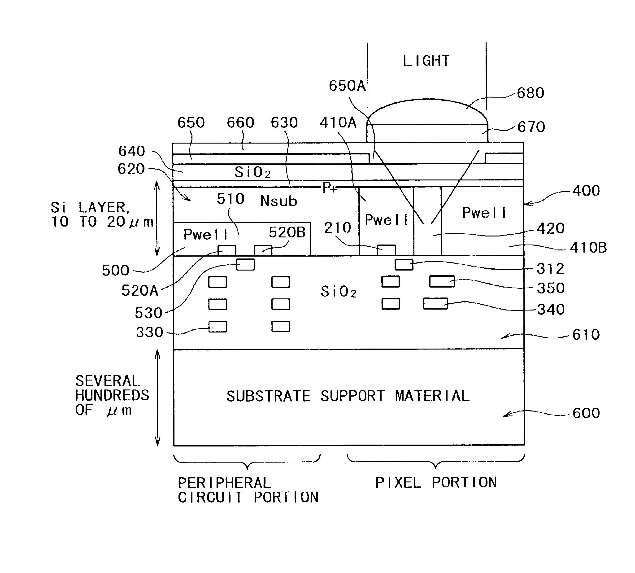
Now, an exemplary embodiment of the method of producing a solid state image pickup device according to the present invention will be described below.

According to the present exemplary embodiment, in the step of producing a back-illuminated type solid state image pickup device for coping with a new generation of process, a registration mark is formed on the wiring side by diverting an active region or a gate electrode (polysilicon film) for use in the step of forming a MOS transistor, for example, in order to conduct registration for a stepper.

In addition, in order to form the registration mark, a silicide film used at the active region may also be used, and the silicide film may be left on photodiodes (on the side opposite to the illuminated side).

Thereafter, registration of the stepper is conducted by reading the registration mark with red light or near infrared rays from the back side.

Incidentally, it is possible to form a registration mark on a silicon oxide film on the back side...


PUM


Abstract

Forming a back-illuminated type CMOS image sensor, includes process for formation of a registration mark on the wiring side of a silicon substrate during formation of an active region or a gate electrode. A silicide film using an active region may also be used for the registration mark. Thereafter, the registration mark is read from the back side by use of red light or near infrared rays, and registration of the stepper is accomplished. It is also possible to form a registration mark in a silicon oxide film on the back side (illuminated side) in registry with the registration mark on the wiring side, and to achieve the desired registration by use of the registration mark thus formed.

Description

This application claims priority to Japanese Patent Application Number JP2002-076081 dated Mar. 19, 2002, which is incorporated herein by reference.The present invention relates to a Solid State Image Pickup Device and a method of producing a solid state image pickup device for use as various kinds of image sensors and camera modules.RELATED ARTIn recent years, the demand for video cameras and electronic cameras has increased dramatically and these cameras use a CCD type or amplification type solid state image pickup device.Among these, the amplification type solid state image pickup device (CMOS image sensor) includes on a single semiconductor chip an image pickup pixel portion comprising a plurality of pixels arranged in a two-dimensional form, and a peripheral circuit portion disposed on the outside of the image pickup pixel portion. In each pixel of the image pickup pixel portion, floating diffusion (FD) portion as well as various MOS transistors including a transfer transistor ...

Claims


Application Information

Patent Timeline
Patent Type & Authority Patents(United States)
IPC IPC(8): H01L23/544H01L21/027H01L27/14H01L27/146H04N5/335H04N5/369H04N5/374
CPCH01L23/544H01L27/1464H01L27/14609H01L27/14625H01L27/14632H01L27/14636H01L27/14683H01L27/14685H01L27/14687H01L31/02162H01L31/0232H01L27/14603H01L27/14643H01L2223/54426H01L2223/54453H01L2924/0002H01L2924/00H01L27/14607H01L27/14612H01L27/1462H01L27/14623H01L27/14627H01L27/1463H01L31/02327
Inventor ABE, TAKASHINAKAMURA, NOBUOMABUCHI, KEIJIUMEDA, TOMOYUKIFUJITA, HIROAKIFUNATSU, EIICHISATO, HIROKI
Owner SONY CORP
Why Eureka
Try Eureka