Platinum silicide permeation layer device with microlocations

a technology of permeation layer and microlocation, which is applied in the direction of liquid gas reaction process, biomass after-treatment, nucleotide library, etc., can solve the problems of permeation layer peeling (lifting), loss of consistency in permeation layer performance, and prone to separation or ‘delaminate’ of membranes from the electrode surface, etc., to achieve robust permeation layer, increase current density, and increase the effect of transport efficiency of charged molecules

Inactive Publication Date: 2005-01-04
ADOR DIAGNOSTICS SRL
View PDF83 Cites 22 Cited by
  • Summary
  • Abstract
  • Description
  • Claims
  • Application Information

AI Technical Summary

Benefits of technology

where R is the electrical resistance of the medium between the anode and the cathode. In systems where a permeation layer is present over such electrodes, the value of R is greatly determined by the physical and chemical nature of said permeation layer. Thus, according to formula (1), the difference between the electronic potentials applied to the electrodes is directly proportional to the intensity or density of the electric current which flows through them. The invention described in this Letters Patent uses a relationship between electric current and voltage wherein electric current densities are at least 0.04 nA/μm2 and/or voltage drops are between 1 and 3 V. The electric current density is defined as the electric current divided by the area of the electrode used to support it.
Additionally, the effectiveness of the translocation of charged biomolecules such as nucleotide oligomers within an electronically-driven system such as that described herein depends on the generation of the proper gradient of positively and negatively charged electrochemical species by the anode and cathode, respectively. For example, effective nucleic acid (i.e. either DNA or RNA) transport may be accomplished by generation of protons and hydroxyl anions when the potential at the anode is greater than +1.29 V with respect to a ‘saturated calomel electrode’ (SCE). When subjected to such demandi

Problems solved by technology

Although materials such as those noted above have been found useful in the role of a porous membrane having desired qualities, it has been found that because of the methodologies commonly used to layer such membranes onto the microchip substrate, the membranes are prone to separate or ‘delaminate’ from the electrode surface.
It is believed this delamination is caused by a change in the chemical make-up at the interface between the permeation layer and the electrode resulting from the application of electronic potential at the electrode and by physical disruption from charged ions and gases emanating from the electrode.
It is observed by the formation of raised bulges in the permeation layer, or by ringlets visible due to defraction of light from the delaminated layer when appropriately viewed by a conf

Method used


Image

  • Platinum silicide permeation layer device with microlocations
  • Platinum silicide permeation layer device with microlocations
  • Platinum silicide permeation layer device with microlocations

Examples


example 1

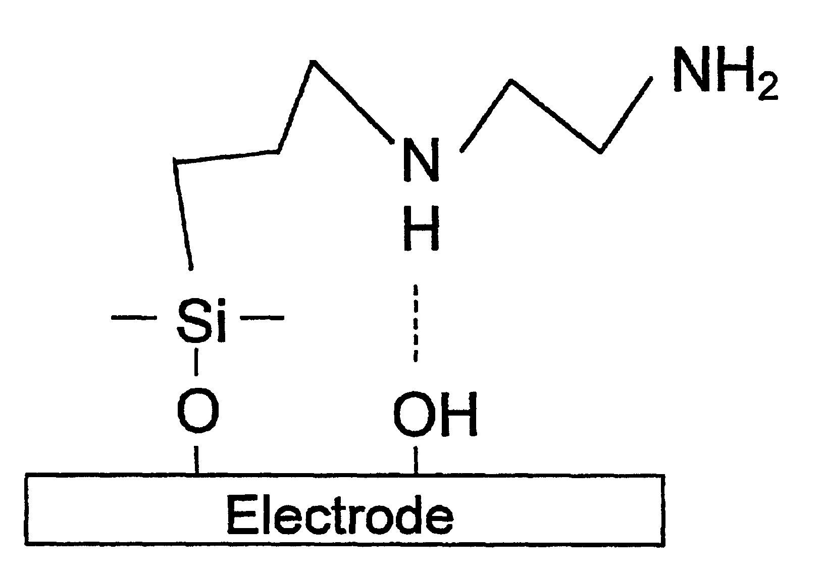
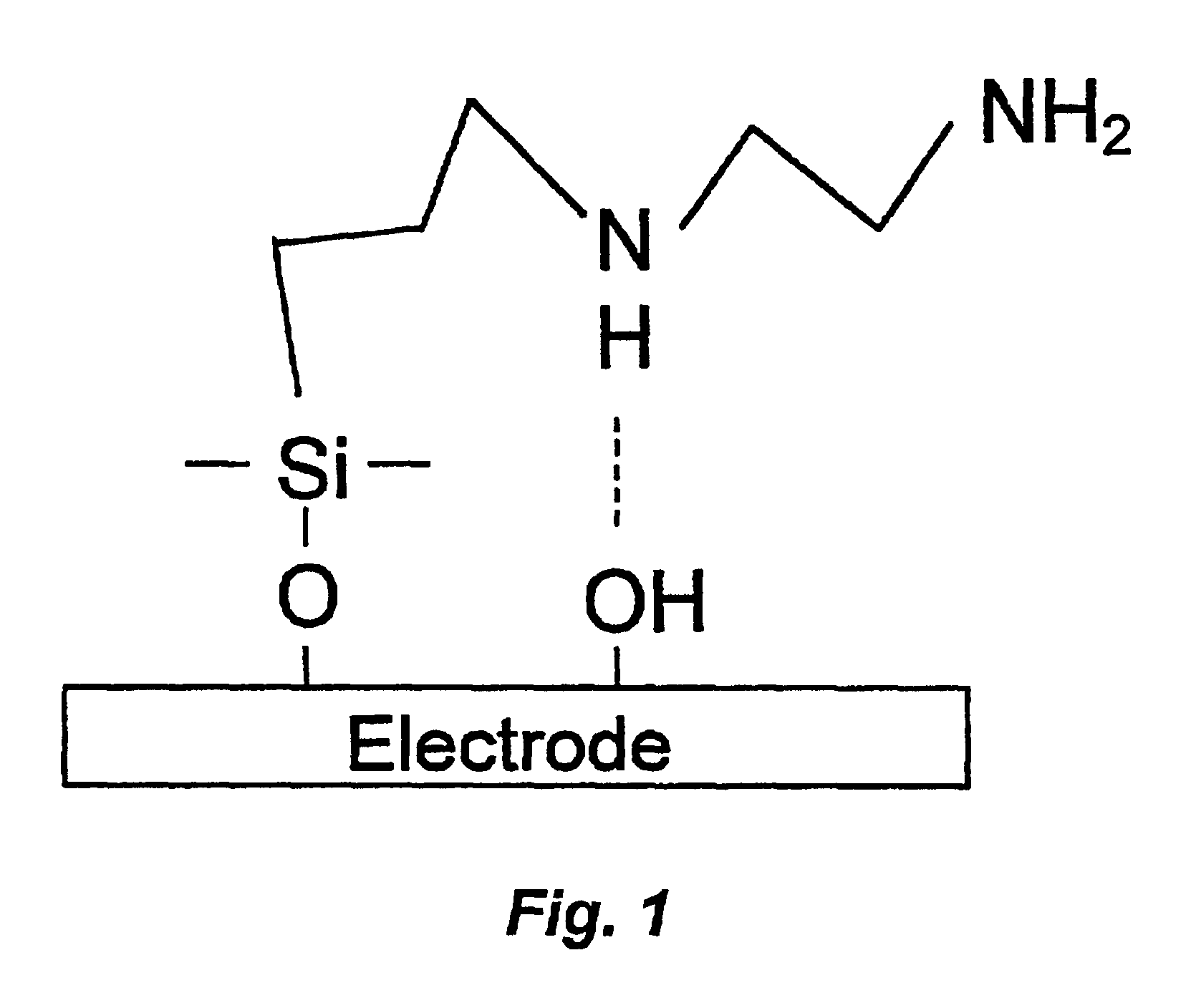
Agarose permeation layer matrix was attached to a PtSi electrode microchip following deposition of either APS or AEAPS by one of two methodologies.

APS and AEAPS were deposited by exposure of the chip to a 0.1 wt % silane / dry MeOH solution for 1 hour at room temperature. The chips were rinsed in EtOH and cured at 90° C. for 1 hour. In parallel experiments, APS and AEAPS linkers were deposited onto microchips by a vapor of neat silane in humid atmosphere for 5 min. at room temperature followed by a two hour cure at 90° C.

After the agarose permeation layer was attached, the microchips were subjected to electronic assays wherein the electrodes were biased with three direct current (DC) impulses for 2 minutes each at 200, 500, 700, and 1000 nAmps / 80 μm pad (i.e., 0.04, 0.10, 0.14 and 0.20 nA / μm2) using a model 236 Source-Measure unit (Keithley Instruments Inc., Cleveland, Ohio). Following the set of three DC impulses, the electrodes were biased with a sequence of 150 negative pulses, eac...

example 2

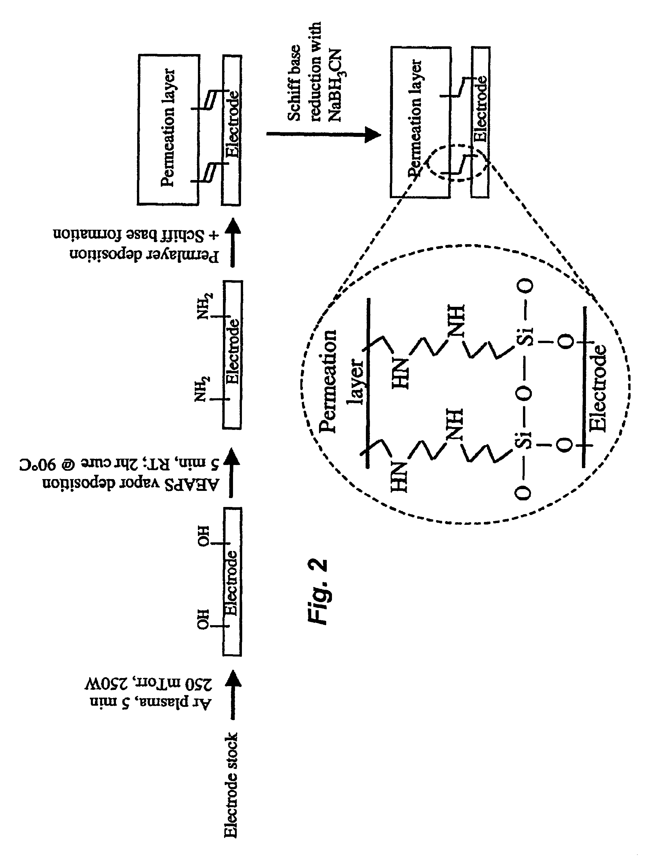
In this example, delamination of the permeation layer from the electrode was tested using a multilayer permeation layer wherein the layers were applied using spin coating techniques then reacted to cause the linking moieties to covalently bond the layers together and to the electrode.

Specifically, microchips having PtSi electrodes were cleaned with oxygen plasma for 10 minutes followed by argon plasma for 10 minutes. AEAPS was then vapor-deposited for 5 minutes followed by curing at 90° C. under vacuum. Subsequently, a first layer solution comprising 2.5% glyoxylagarose solution (NuFix) which had been stirred for 10 minutes at room temperature then boiled 7 minutes followed by filtering at 1.2 μm into the ASC device reservoir at 65° C., was spin-deposited onto the microchips with an automatic spin-coating device (ASC). Following deposition of the first layer, a second layer, comprising streptavidin (Scripps Laboratory, San Diego) at 5 mg / ml in 10 mM sodium phosphate, 250 mM NaCl (pH...

example 3

In this example, data is presented showing that the covalent attachment method of the invention using PtSi electrodes, agarose and aminopropylsilanes also protects against delamination of the permeation layer under alternating current conditions. Here, Pt and PtSi microchips bonded to the permeation layer with AEAPS were tested using two pulsed biasing protocols.

Both protocols were carried out using 50 mM L-Histidine buffer. Specifically, in protocol A, the microchips were biased at +800 nA / pad (0.16 nA / μm2) for 38 milliseconds (ms), −800 nA / pad for 25 ms, cycled for a total of 25 seconds using 3 pads each pulse. In protocol B, the microchips were biased at +1.6 μA / pad (0.32 nA / μm2) for 19 ms, −1.6 μA / pad for 12 ms, and cycled for a total of 14 seconds each on 3 pads addressed simultaneously. Images were taken using an INM 100 confocal microscope (Leica).

FIG. 6A shows Pt chips that were biased using protocol A, followed by 0, 4, 8, 12 or 16 repeats of protocol B. The images show tha...


PUM

PropertyMeasurementUnit
Current densityaaaaaaaaaa

Abstract

Electronically addressable microchips having covalently bound permeation layers and methods of making such covalently bonded permeation layers to microchips are provided. The covalent bonding is derived from combining the use of electrodes with silane derivatives. Such chemistry provides the ability to apply an electronic bias to the electrodes of the microchip while preventing permeation layer delaminating from the electrode surface.

Description

FIELD OF THE INVENTIONThis invention relates to the attachment of a layer of polymeric material to a substrate surface. More particularly, this invention relates to chemistries and methods for covalently attaching a porous polymeric material to an electrically conductive substrate, such as a metal electrode of a microchip circuit.BACKGROUND OF THE INVENTIONThe following description provides a summary of information relevant to the present invention. It is not an admission that any of the information provided herein is prior art to the presently claimed invention, nor that any of the publications specifically or implicitly referenced are prior art to the invention.In the art of electronically addressable microchips that are used to direct biomaterials, such as nucleic acids and proteins, from one point in a solution to another, the microchips should be designed so that electric potential from the microchip electrodes will translate to the solution overlying the microchip such that an...

Claims


Application Information

Patent Timeline
IPC IPC(8): G01N27/40G01N33/543G01N33/53C40B40/06C40B40/10G01N37/00
CPCG01N33/5438G01N27/40B01J2219/00653B01J2219/00659B01J2219/00722C40B40/06C40B40/10B01J2219/00725G01N33/48
Inventor JOHN, HAVENS R.WINGER, THEODORE M.KROTZ, JAINDAN, SMOLKOONOFREY, THOMAS J.
Owner ADOR DIAGNOSTICS SRL
Why Eureka
Try Eureka