Substrate assembly for electrooptical device, method for manufacturing substrate assembly for electrooptical device, electrooptical device, method for manufacturing electrooptical device, and electronic apparatus

a technology for electrooptical devices and substrates, applied in the direction of mirrors, instruments, identification means, etc., can solve the problems of insufficient chroma, user's perception of color tone, and lack of brightness of reflective-type displays, so as to improve the quality of color presentation in the reflective region and the transmissive region, and avoid the thickness of the color filter. uniform

Inactive Publication Date: 2005-02-01
BOE TECH GRP CO LTD
View PDF22 Cites 13 Cited by
  • Summary
  • Abstract
  • Description
  • Claims
  • Application Information

AI Technical Summary

Benefits of technology

To satisfy the flatness and the optical characteristics of the color filter at the same time, the mean thickness of the thick portion of the color filter overlapping the aperture of the reflective layer preferably falls within a range from 1.0 to 3.0 μm, and the thickness of the color layer in the area thereof overlapping the reflective layer surrounding the aperture (the thickness of the color layer other than the aperture) preferably falls within a range of 0.2 to 1.5 μm. In this arrangement, the non-uniformity in the thickness of the color filter due to the presence of the thick portion thereof is reduced and the quality of the color presentation in the reflective region and the transmissive region is improved.

Problems solved by technology

Specifically, the reflective-type display typically tends to suffer from the lack of brightness.
A high light transmittance in the transmissive display means insufficient chroma.
As a result, the user may feel odd about color tone.

Method used


Image

  • Substrate assembly for electrooptical device, method for manufacturing substrate assembly for electrooptical device, electrooptical device, method for manufacturing electrooptical device, and electronic apparatus
  • Substrate assembly for electrooptical device, method for manufacturing substrate assembly for electrooptical device, electrooptical device, method for manufacturing electrooptical device, and electronic apparatus
  • Substrate assembly for electrooptical device, method for manufacturing substrate assembly for electrooptical device, electrooptical device, method for manufacturing electrooptical device, and electronic apparatus

Examples


first embodiment

[First Embodiment]

The electrooptical device of a first embodiment of the present invention will be discussed with reference to FIG. 1 and FIG. 2.

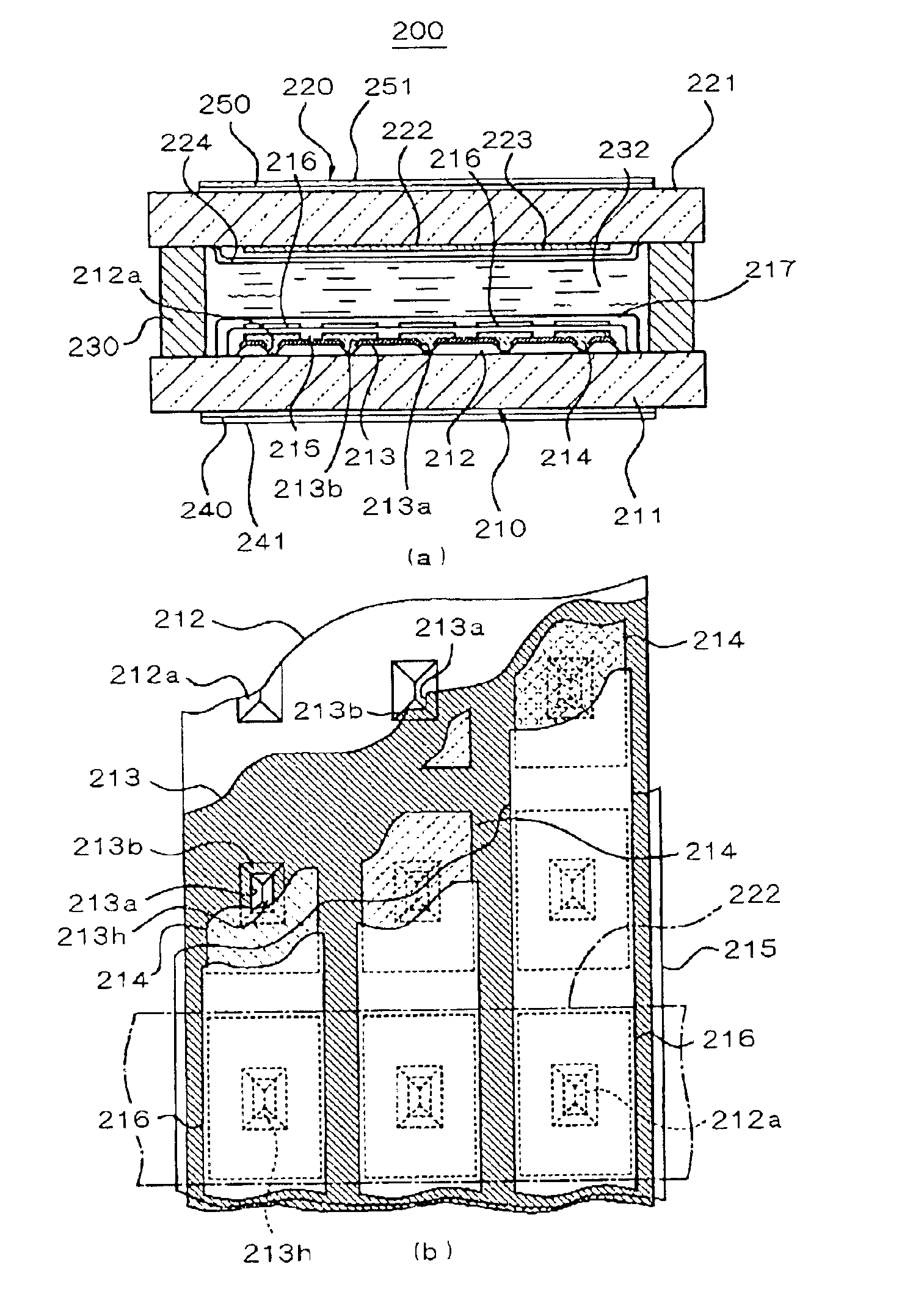
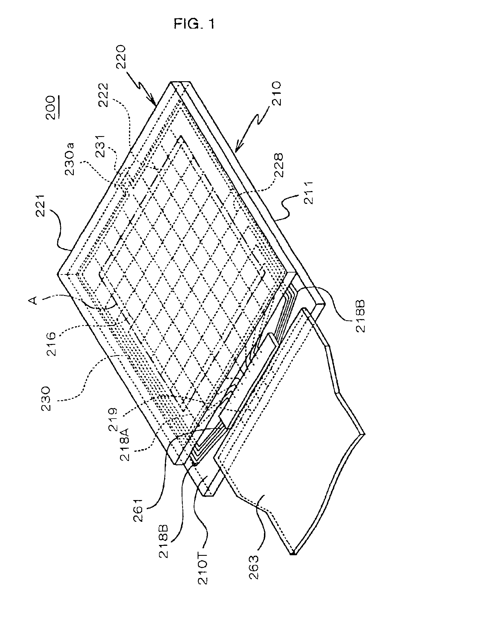
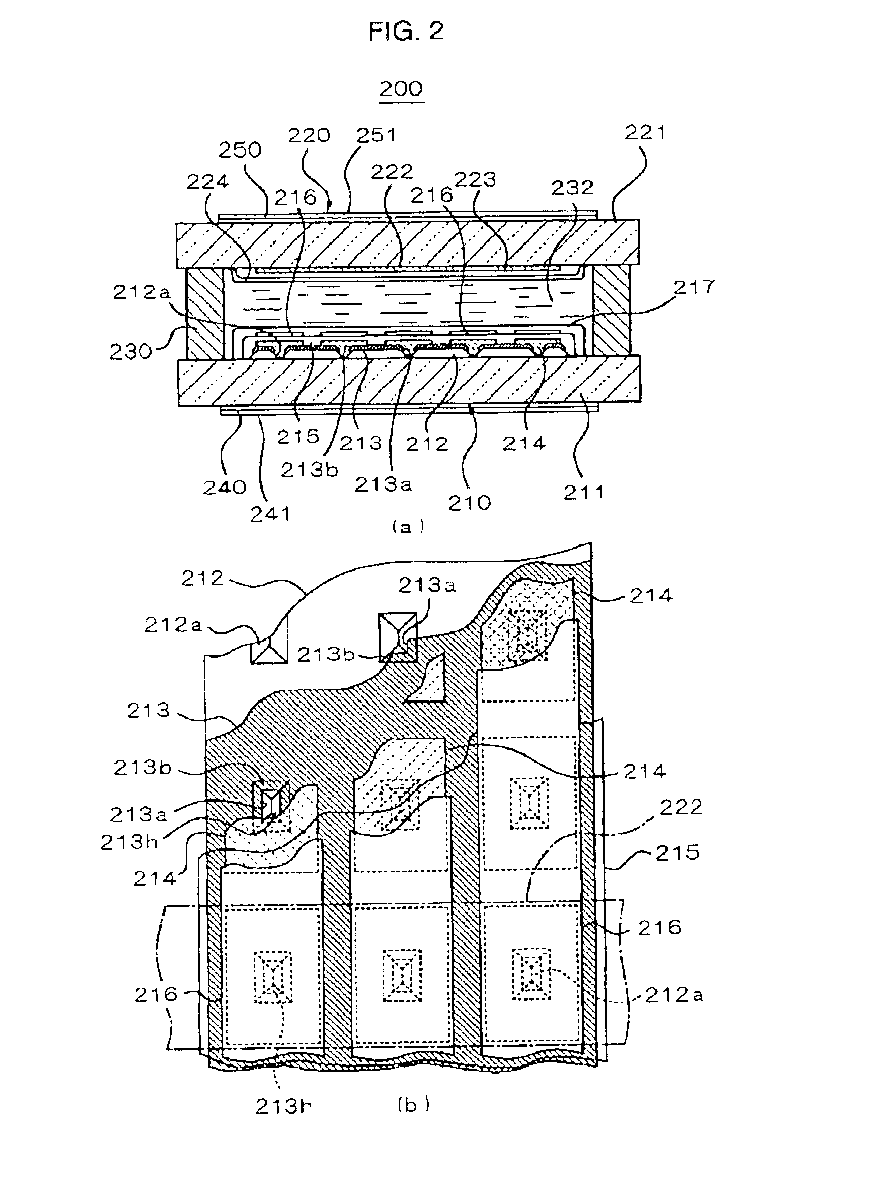
FIG. 1 is a diagrammatic external perspective view illustrating a liquid-crystal panel 200 forming a liquid-crystal device in accordance with the first embodiment of the present invention. FIG. 2(a) is a diagrammatic perspective view of the liquid-crystal panel 200, and FIG. 2(b) is an enlarged plan view illustrating a portion of a color filter substrate 210 forming the liquid-crystal panel 200.

The liquid-crystal device includes a reflective-type passive-matrix liquid-crystal panel 200, an unshown illumination device such as an unshown backlight or a front light and a case attached to the liquid-crystal panel 200.

Referring to FIG. 1, the liquid-crystal panel 200 includes a color filter substrate 210 including, as a base body, a first transparent substrate 211 fabricated of a glass plate or a synthetic resin plate, and a counter substrate 22...

second embodiment

[Second Embodiment]

Referring to FIGS. 4(a) and 4(b), the construction of the liquid-crystal panel 200′ of a second embodiment of the present invention is discussed below. The liquid-crystal panel 200′ has a construction substantially identical to that of the liquid-crystal panel 200. As in the first embodiment, the liquid-crystal panel 200′ includes, on the color filter substrate 210, the first substrate 211, the optically transmissive layer 212, the color layer 214, the surface protective layer 215, the transparent electrodes 216, the alignment layer 217, and the second substrate 221 and the hard protective layer 223, and the alignment layer 224 on the counter substrate 220. Furthermore, as in the first embodiment, the liquid-crystal panel 200′ includes the sealing member 230, the liquid crystal 232, the retardation films 240 and 250, and the polarizers 241 and 251. The description thereof is omitted here.

In this embodiment, one reflective layer 213′ formed on the optically transmi...

third embodiment

[Third Embodiment]

Referring to FIGS. 5(a)-5(e), the manufacturing process of the color filter substrate 210 is discussed below, which is applicable to the method for manufacturing the liquid-crystal device of the present invention, or the method for manufacturing the substrate assembly for the liquid-crystal device of the present invention.

Referring to FIG. 5(a), an optically transmissive layer 212X is formed entirely on the surface of the first substrate 211. The optically transmissive layer 212X, fabricated of a transparent resin such as acrylic resin or epoxy resin, is applied and then dried.

Referring to FIG. 5(b), an aperture 212Y is formed in the optically transmissive layer 212X on the first substrate 211 for each pixel using the photolithographic technique and etching process. The optically transmissive layer 212X is then softened to be flowable through a heat treatment, and the slope surface 212a is formed in the vicinity of the edge of the aperture 212Y with reference to FI...


PUM

PropertyMeasurementUnit
inclination angleaaaaaaaaaa
thicknessaaaaaaaaaa
thicknessaaaaaaaaaa

Abstract

An optically transmissive layer 212 is formed on a first substrate 211, and a slope surface 212a having a valley in cross section is formed in the optically transmissive layer 212. A reflective layer 213 having a aperture 213h on the slope surface 212a is formed on the optically transmissive layer 212. A color layer 214 is formed on the reflective layer 213. The color layer 214 has a thick portion 214a formed corresponding to the slope surface 212a of the optically transmissive layer 212.

Description

BACKGROUND OF THE INVENTION1. Technical Field of the InventionThe present invention relates to a substrate assembly for an electrooptical device, a method for manufacturing the substrate assembly for the electrooptical device, the electrooptical device, and a method for manufacturing the electrooptical device, and, more particularly, to a structure and a manufacturing process technology appropriate for a transflective-type liquid-crystal device.2. Description of the Related ArtA transflective-type liquid-crystal display panel presenting both a reflective-type display using external light and a transmissive-type display using illumination light such as the one from a backlight is known. The transflective-type liquid-crystal display panel includes a reflective layer which reflects external light into the panel while transmitting illumination light from a backlight or the like. This type of reflective layer includes an aperture (a slit) having a predetermined area at each pixel of a li...

Claims


Application Information

Patent Timeline
Patent Type & Authority Patents(United States)
IPC IPC(8): G02F1/1335G02F1/13G02B5/02G02B5/08G02B5/20G02F1/1333G09F9/00G09F9/30G09F9/35
CPCG02F1/133555G02F1/1333
Inventor TAKIZAWA, KEIJIOTAGIRI, YOSHIHIRO
Owner BOE TECH GRP CO LTD
Why Eureka
Try Eureka