Liquid crystal device and electronic apparatus

a liquid crystal device and electronic device technology, applied in non-linear optics, instruments, optics, etc., can solve the problems of difficult spacer function as spacer, and difficult to form spacer on embedded retardation film, so as to prevent deterioration of display quality, and eliminate the effect of thickness non-uniform alignment layer

Active Publication Date: 2013-12-03
JAPAN DISPLAY WEST
View PDF34 Cites 0 Cited by
  • Summary
  • Abstract
  • Description
  • Claims
  • Application Information

AI Technical Summary

Benefits of technology

[0012]An advantage of some aspects of the invention is to provide a liquid crystal device which makes it possible to dispose a spacer for setting a distance between substrates, to prevent deterioration of display quality by eliminating thickness non-uniformity of an alignment layer due to the presence of a retardation layer, to prevent deterioration of display quality by preventing dissolution and flow of an ingredient of the retardation layer to the liquid crystal layer side, and the like in the liquid crystal device having a horizontal electric field system of a transflective type, and to provide an electric apparatus using the same.

Problems solved by technology

Accordingly, the embedded retardation film is generally soft, so that it is difficult to form the spacer on the embedded retardation film.
Even when the spacer can be formed on the retardation film, there is a problem in that it is difficult for the spacer to function as a spacer due to the softness.
This causes thickness non-uniformity of the alignment layer.
Consequently, there is a problem in that line display non-uniformity occurs due to the thickness non-uniformity of the alignment layer to deteriorate display quality.
Further, in the liquid crystal device, the thickness of the alignment layer is generally thin.
Accordingly, there is a problem in that an ingredient of the embedded retardation film is dissolved to flow to the liquid crystal layer through the alignment layer to deteriorate display quality.
Accordingly, the retardation layer is generally soft, so that it is difficult to form the spacer on the retardation layer.
Even when the spacer can be formed on the retardation layer, it is difficult for the spacer to function as a spacer due to the softness.
Consequently, in the comparative example, there is a problem in that line display non-uniformity occurs due to the thickness non-uniformity of the alignment layer.
Herein, when the spacer is provided near the slit of the retardation layer or on the extended line in the extending direction of the slit, there is a fear in that the flow of the alignment layer through the slit between one transmissive display area and the other transmissive display area provided at the position to sandwich the reflection display area may be stopped when forming the alignment layer for setting the alignment of the liquid crystal layer at the second substrate side.
Generally, the thickness of the alignment layer formed on the retardation layer is thin, so that there is a fear in that an ingredient contained in the retardation layer is dissolved to flow to the liquid crystal layer side through the alignment layer due to the thickness to deteriorate display quality.

Method used


Image

  • Liquid crystal device and electronic apparatus
  • Liquid crystal device and electronic apparatus
  • Liquid crystal device and electronic apparatus

Examples


first embodiment

Structure of Liquid Crystal Device

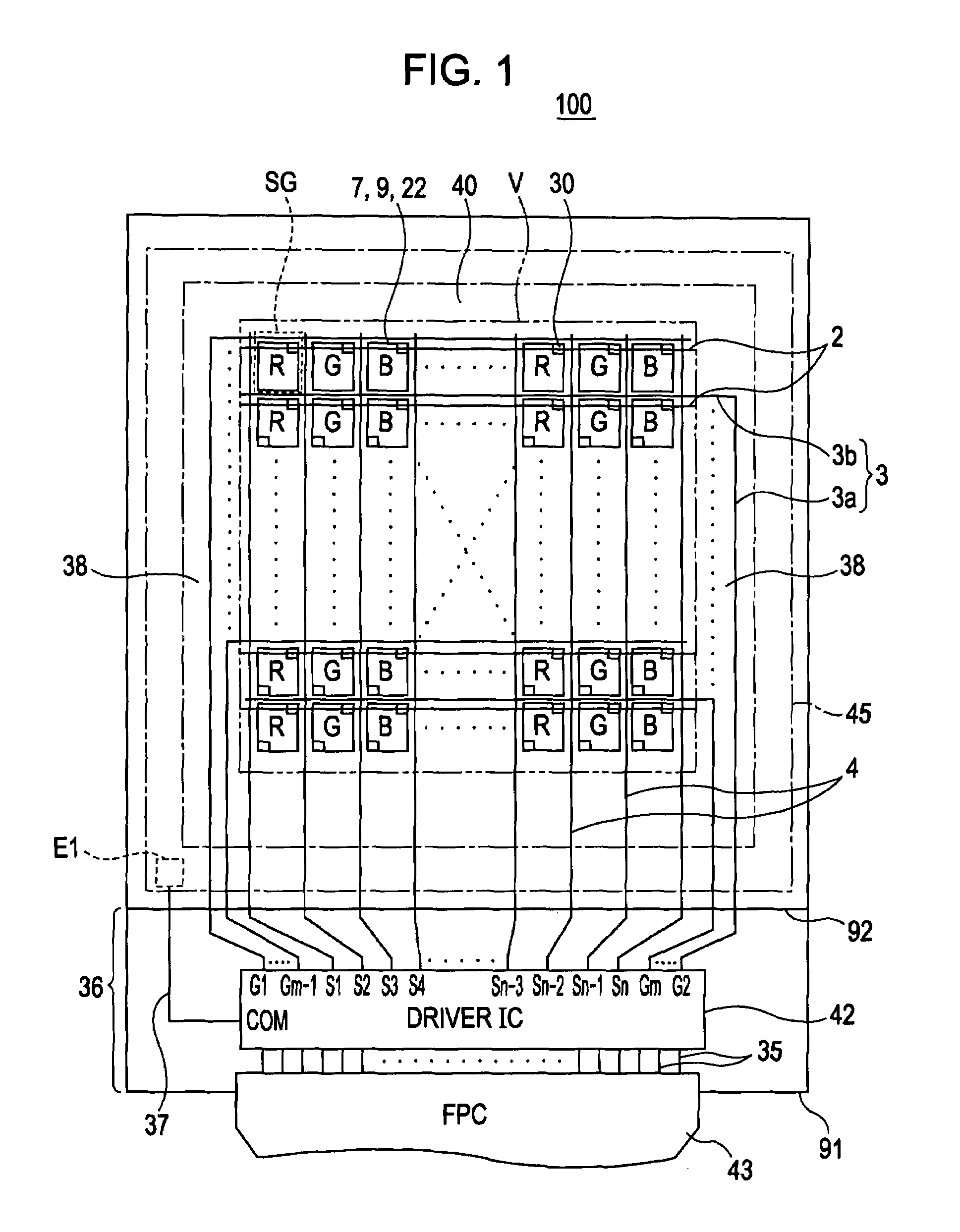
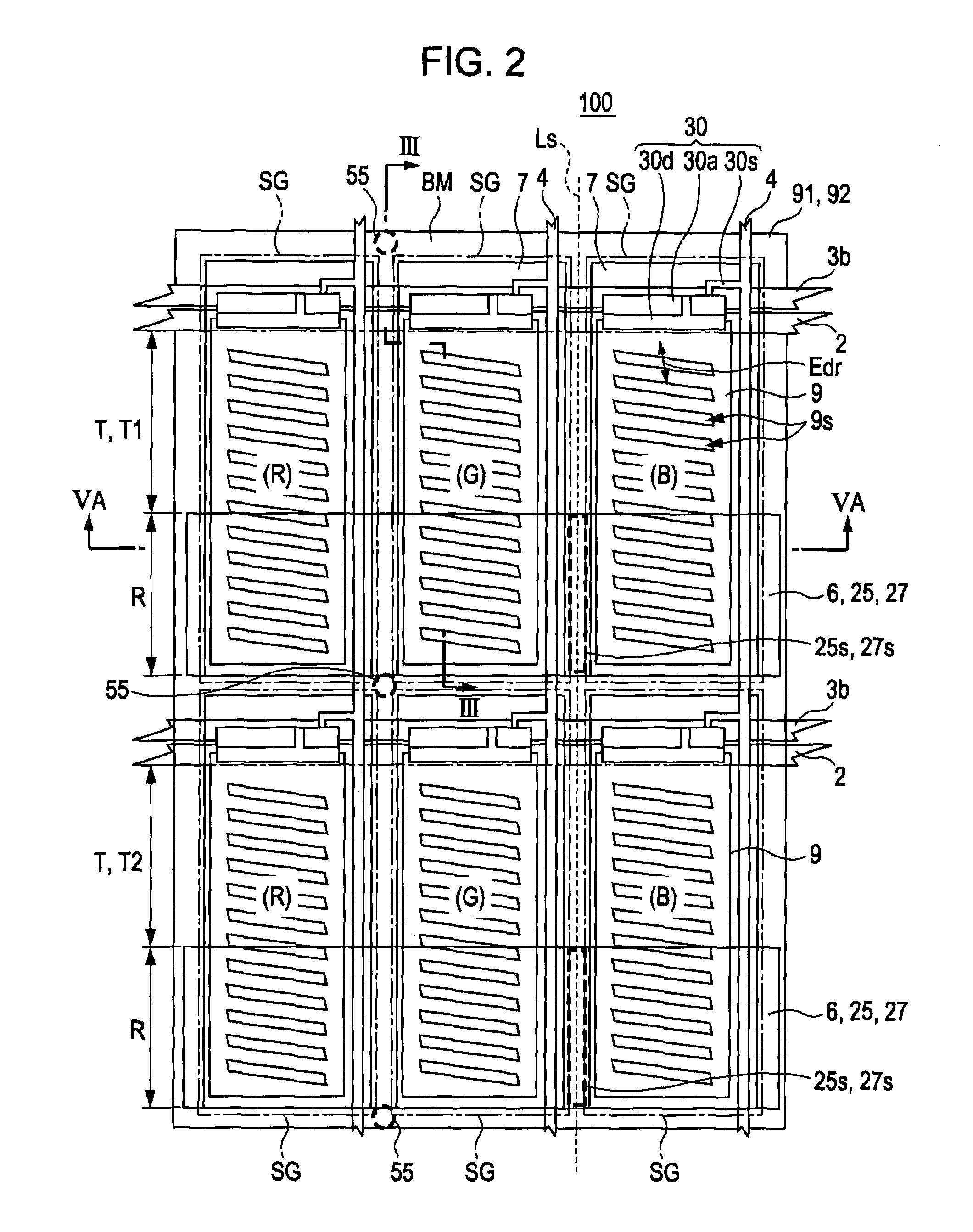
[0050]First, a planar structure focusing on an electrode and a wiring structure of a liquid crystal device according to a first embodiment of the invention will be described with reference to FIG. 1.

[0051]FIG. 1 is a plan view schematically showing an electrode and a wiring structure of the liquid crystal device according to the first embodiment. In FIG. 1, a color filter substrate 92 and an element substrate 91 are respectively disposed at the front side of the paper surface (observation side) and the rear side of the paper surface. Further, in FIG. 1, the overlapping area of the area corresponding to each of coloring layers 22 of R, G, B three colors having a rectangular plan shape provided at the color filter substrate 92 side and each pixel electrode 9 provided at the element substrate 91 side shows one sub pixel area (a sub pixel area) SG which becomes the minimum unit for display. The area in which a plurality of sub pixel areas SG are aligned...

second embodiment

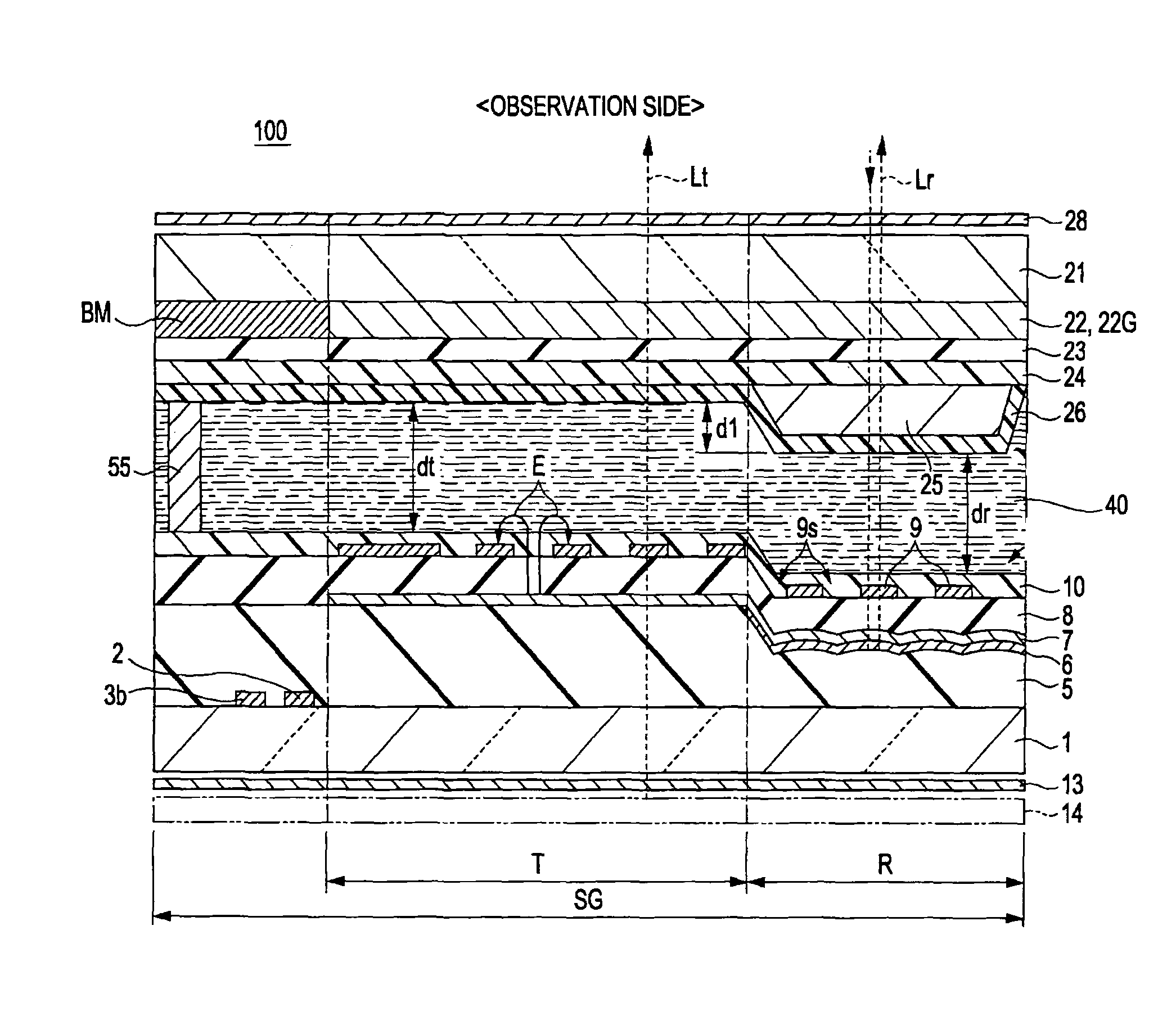
[0097]Next, a structure of a color filter substrate 94 according to a second embodiment of the invention will be described with reference to FIG. 6A and the like. FIG. 6A is a cross sectional view showing the color filter substrate 94 according to the second embodiment of the invention corresponding to FIG. 5A.

[0098]When comparing the second embodiment with the first embodiment, in the second embodiment, a protection layer 27 is further provided between the retardation layer 25 and the second alignment layer 26 in the reflective display area R at the color filter substrate 94 side and the pint only is different from the first embodiment in the structure. Accordingly, the same reference numeral is used to denote the same element as that in the first embodiment and further description thereof will be omitted.

[0099]Generally, the thickness of the second alignment layer 26 formed on the retardation layer 25 is thin, so that there is a fear in that an ingredient contained in the retardat...


PUM

PropertyMeasurementUnit
angleaaaaaaaaaa
angleaaaaaaaaaa
electric fieldaaaaaaaaaa

Abstract

A liquid crystal device in which a horizontal electric field is applied to a liquid crystal layer of a transflective type. Spacers are disposed to set a distance between substrates and to prevent deterioration of display quality by eliminating thickness non-uniformity of an alignment layer due to the presence of a retardation layer. Slits are provided in the retardation layer regions to prevent deterioration of display quality by preventing dissolution and flow of an ingredient of the retardation layer to the liquid crystal layer side through the alignment layers.

Description

[0001]The entire disclosure of Japanese Patent Application No. 2007-061334, filed Mar. 12, 2007 is expressly incorporated by reference herein.BACKGROUND[0002]1. Technical Field[0003]The present invention relates to a liquid crystal device preferably used for displaying various information.[0004]2. Related Art[0005]Currently, a liquid crystal device of a horizontal electric field system represented by an IPS (In-Plane Switching) system and an FFS (Fringe Field Switching) system are preferably used as various display devices such as a mobile apparatus. The horizontal electric field system is a system in which a direction of an electric field applied to liquid crystal is set approximately parallel to a substrate and there is an advantage in that wide viewing angle property can be obtained as compared with a TN (Twisted Nematic) system or the like.[0006]An example in which such a horizontal electric field system which can obtain wide viewing angle property is applied to a transflective ...

Claims


Application Information

Patent Timeline
Patent Type & Authority Patents(United States)
IPC IPC(8): G02F1/1335G02F1/1343
CPCG02F1/133555G02F1/134363G02F1/13394G02F1/133371G02F1/13363G02F2001/134372G02F2001/133565G02F1/133565G02F1/134372G02F1/1335
Inventor HIGA, MASAKATSU
Owner JAPAN DISPLAY WEST
Why Eureka
Try Eureka