Optical connector module

a technology of optical connectors and modules, applied in the field of optical connector modules, can solve problems such as misregistration between wafers, and achieve the effect of preventing misregistration and facilitating registration

Inactive Publication Date: 2005-02-08
JAPAN AVIATION ELECTRONICS IND LTD
View PDF2 Cites 1 Cited by
  • Summary
  • Abstract
  • Description
  • Claims
  • Application Information

AI Technical Summary

Benefits of technology

It is an object of the present invention to provide an optical connector module which facilitates registration between an optical transmission / reception wafer and an optical waveguide wafer thereof, and prevents misregistration between an optical transmission / reception surface of an optical transmission / reception section and an optical transmission / reception surface of an optical waveguide thereof when the wafers are connected to each other.

Problems solved by technology

Therefore, the conventional optical connector module suffers the problem of difficulty of registering the markers 140 and 214 with each other, and what to worse, there to a fear of misregistration occurring between the wafers when they are connected to each other.

Method used


Image

  • Optical connector module
  • Optical connector module
  • Optical connector module

Examples


second embodiment

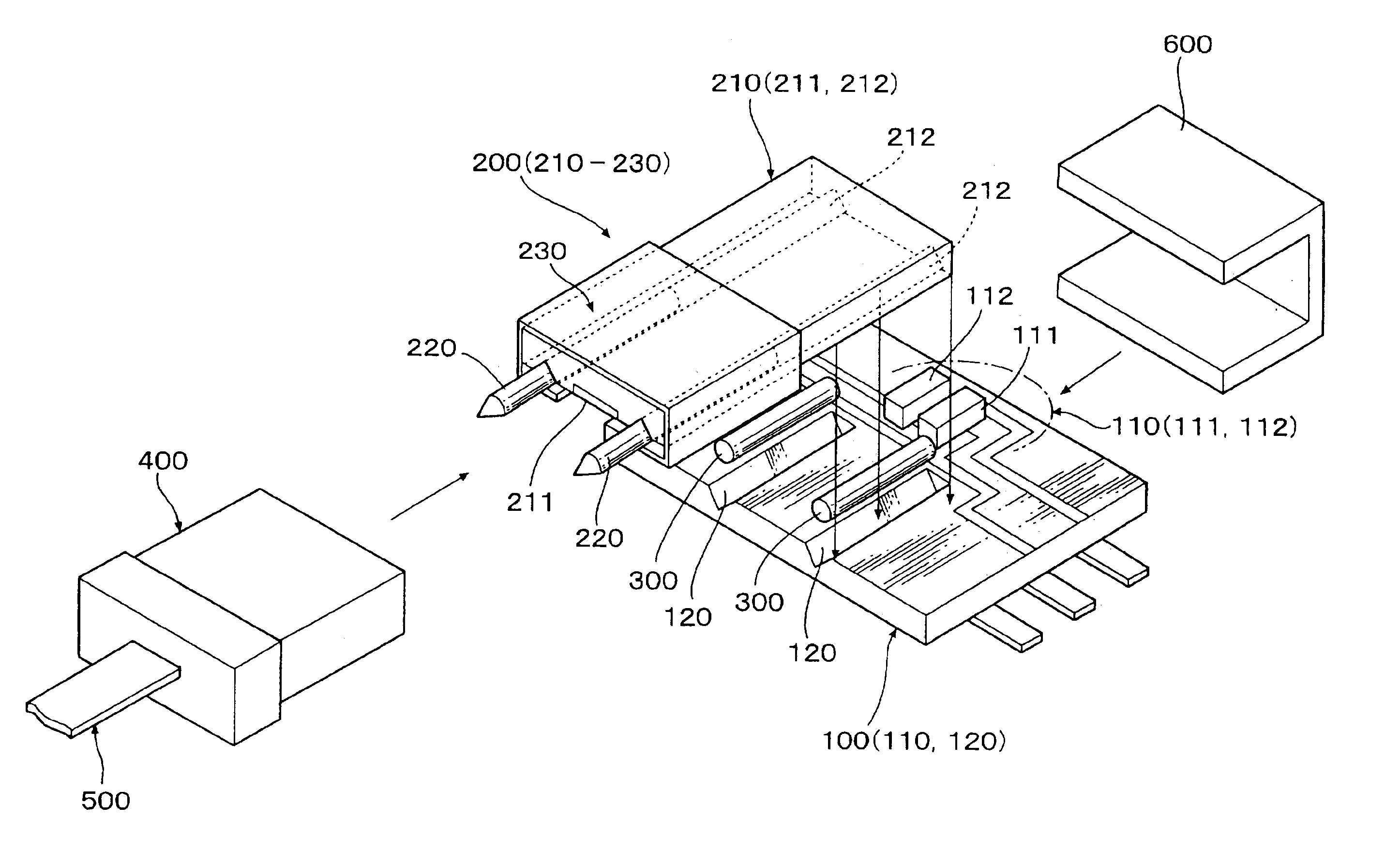
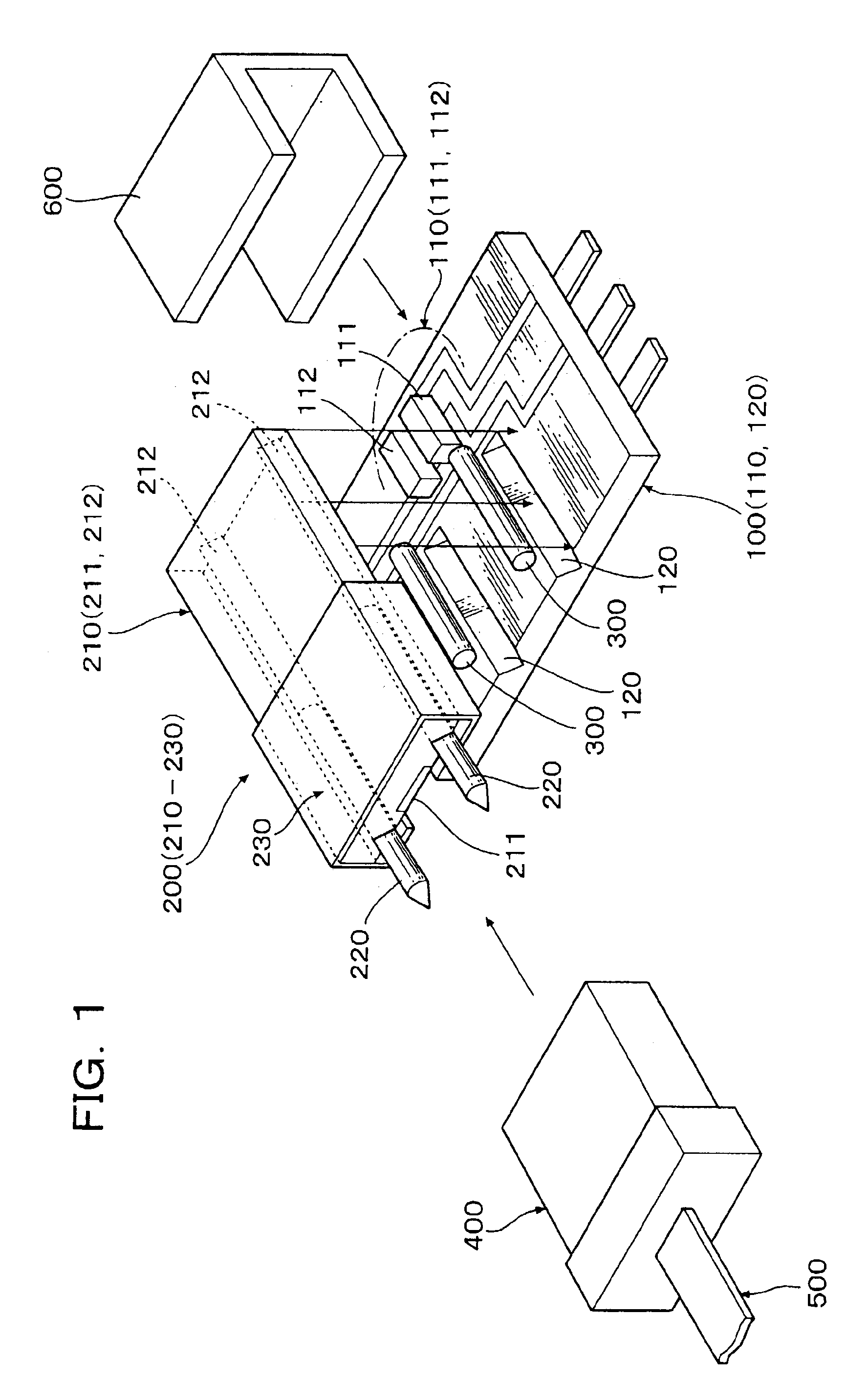
FIG. 2 is an exploded perspective view of an optical connector module according to the present invention.

The second embodiment is distinguished from the first embodiment described above in that the connector guide pins 220, of the optical waveguide-side connector 200 and the wafer registration guide pins 300 in the first embodiment are integrally formed with each other to form guide pins 240, respectively, and the guide pins 240 are received in guide pin-receiving V-grooves 212 of an optical waveguide wafer 210, with connector guide pin-corresponding portions of the guide pins 240 being fixedly held by a pin-fixing member 230, thus forming an optical waveguide-side connector 200a.

According to the second embodiment, since each connector guide pin and each wafer registration guide pin are integrally formed with each other and contained in the optical waveguide-side connector 200a, there is no need to handle the wafer registration guide pins as single separate elements as in the case ...

third embodiment

FIG. 3 to an exploded perspective view of an optical connector module according to the present invention.

This embodiment is distinguished from the above second embodiment in which the guide pins 240 and the guide pin-receiving V-grooves 120, 212 for sandwiching the guide pins 240 are arranged along opposite sides of the optical waveguide 211′, in that there are provided not only guide pins 240a disposed along opposite sides of an optical waveguide 211, and guide pin-receiving V-grooves 120a, 212a for sandwiching the guide pins 240a, but also guide pin-receiving V-grooves 130, 213 which are formed orthogonal to the guide pin-receiving V-grooves 120a, 212a, thus forming an optical transmission / reception wafer 100a and an optical waveguide wafer 210a, with an additional member of an wafer registration guide pin 350 for being sandwiched by the guide pin-receiving V-grooves 130, 213.

The above arrangement and configuration provides the advantageous effects of being capable of uniquely con...

fourth embodiment

FIG. 4 is an exploded perspective view of an optical connector module according to the present invention.

In the fourth embodiment, the integrally-formed guide pins 240a in the third embodiment are divided into connector guide pins 220 and wafer registration guide pins 300a, as in the first embodiment. The arrangement and configuration make it possible to use the wafer registration guide pins 300a having a diameter different from that of the connector guide pins 220, which provides the advantages effect of being capable of controlling registration accuracy, wafer interconnection accuracy, and so forth.

Further, similarly, it is also possible to control registration accuracy, wafer interconnection accuracy, and so forth, based on a diameter of the wafer registration guide pin 350 orthogonal to the wafer registration guide pins 300a. The other advantageous effects provided by the fourth embodiment are the same as those obtained by the third embodiment.


PUM


Abstract

There is provided an optical connector module of which an optical transmission/reception wafer and an optical waveguide wafer can be registered with each other easily and accurately without misregistration. An optical transmission/reception wafer has guide pin-receiving V-grooves with a V-shaped cross-section, formed at locations preset in association with an optical transmission/reception end of an optical transmission/reception section. An optical waveguide-side connector has an optical waveguide wafer formed with guide pin-receiving V-grooves in association with the guide pin-receiving V-grooves of the optical transmission/reception wafer. Wafer registration guide pins are inserted in these guide pin-receiving V-grooves, and the optical transmission/reception wafer and the optical waveguide wafer are brought close for interconnection such that these guide pins are tightly sandwiched by the guide pin-receiving grooves.

Description

BACKGROUND OF THE INVENTIONField of the InventiomThis invention relates to an optical connector module, and more particularly to an optical connector module for connecting between a transmission / reception source circuit and an optical fiber.PRIOR ARTWhen signals are transmitted through an optical fiber, an optical connector module is usually used which has an optical waveguide interposed between a transmission / reception source circuit for transmitting and receiving the signals and the optical fiber. An example of a conventional optical connector module of this kind is illustrated in FIG. 5.The optical connector module is comprised of an optical transmission / reception wafer 100x, an optical waveguide-side connector 200x, an optical fiber-side connector 400, and a coupling / fixing member for coupling and fixing the optical transmission / reception wafer 100x and the optical waveguide-side connector 200x to each other. Detailed description of these components will be given hereafter.First...

Claims


Application Information

Patent Timeline
Patent Type & Authority Patents(United States)
IPC IPC(8): G02B6/36G02B6/42
CPCG02B6/3636G02B6/4292G02B6/4231G02B6/3652G02B6/3692
Inventor KOREEDA, YUICHIKOSHIZUKA, HIROAKIKAKU, RYOJIMASE, TAKAOMIYASHITA, TAKUYA
Owner JAPAN AVIATION ELECTRONICS IND LTD
Why Eureka
Try Eureka