Physically defined varactor in a CMOS process

a technology of cmos and varactor, applied in the field of integrated circuits, can solve the problems of reducing jitter performance, unable to achieve demand standards, and prior art cmos voltage controlled capacitors do not have comparable qs,

Inactive Publication Date: 2005-02-15
INTEL CORP
View PDF1 Cites 13 Cited by
  • Summary
  • Abstract
  • Description
  • Claims
  • Application Information

AI Technical Summary

Problems solved by technology

Such demanding standards may be difficult to achieve with current transceivers implemented in complementary metal oxide semiconductor (CMOS) technology.
Unfortunately, prior art CMOS voltage controlled capacitors do not have comparable Qs because of relatively large parasitic resistance (Reff).
In many instances, the Q of the LC tank is so degraded that it may be unusable in SONET or other high-speed environments having demanding jitter performance standards because the parasitic resistance is a source of noise, which reduces jitter performance.

Method used


Image

  • Physically defined varactor in a CMOS process
  • Physically defined varactor in a CMOS process
  • Physically defined varactor in a CMOS process

Examples


Embodiment Construction

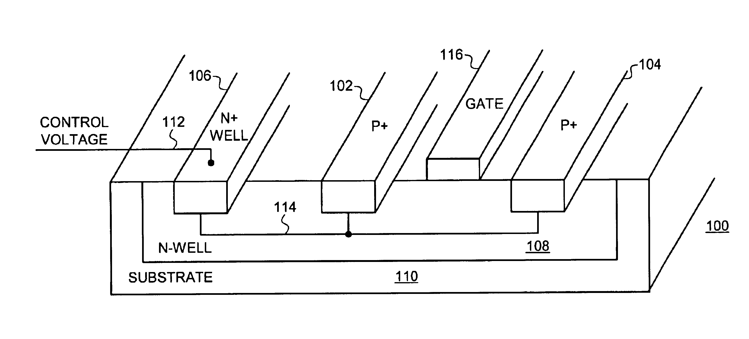
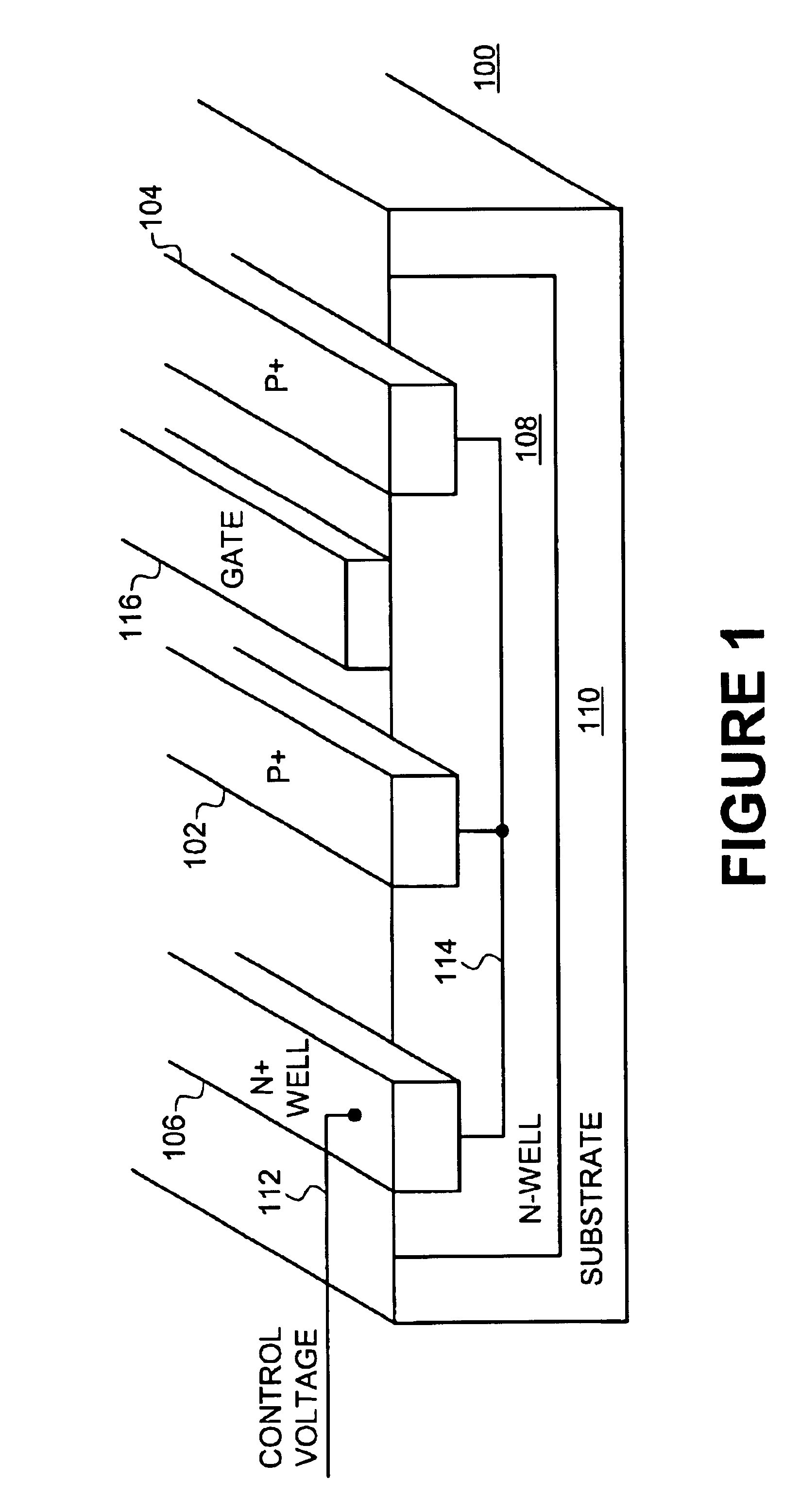
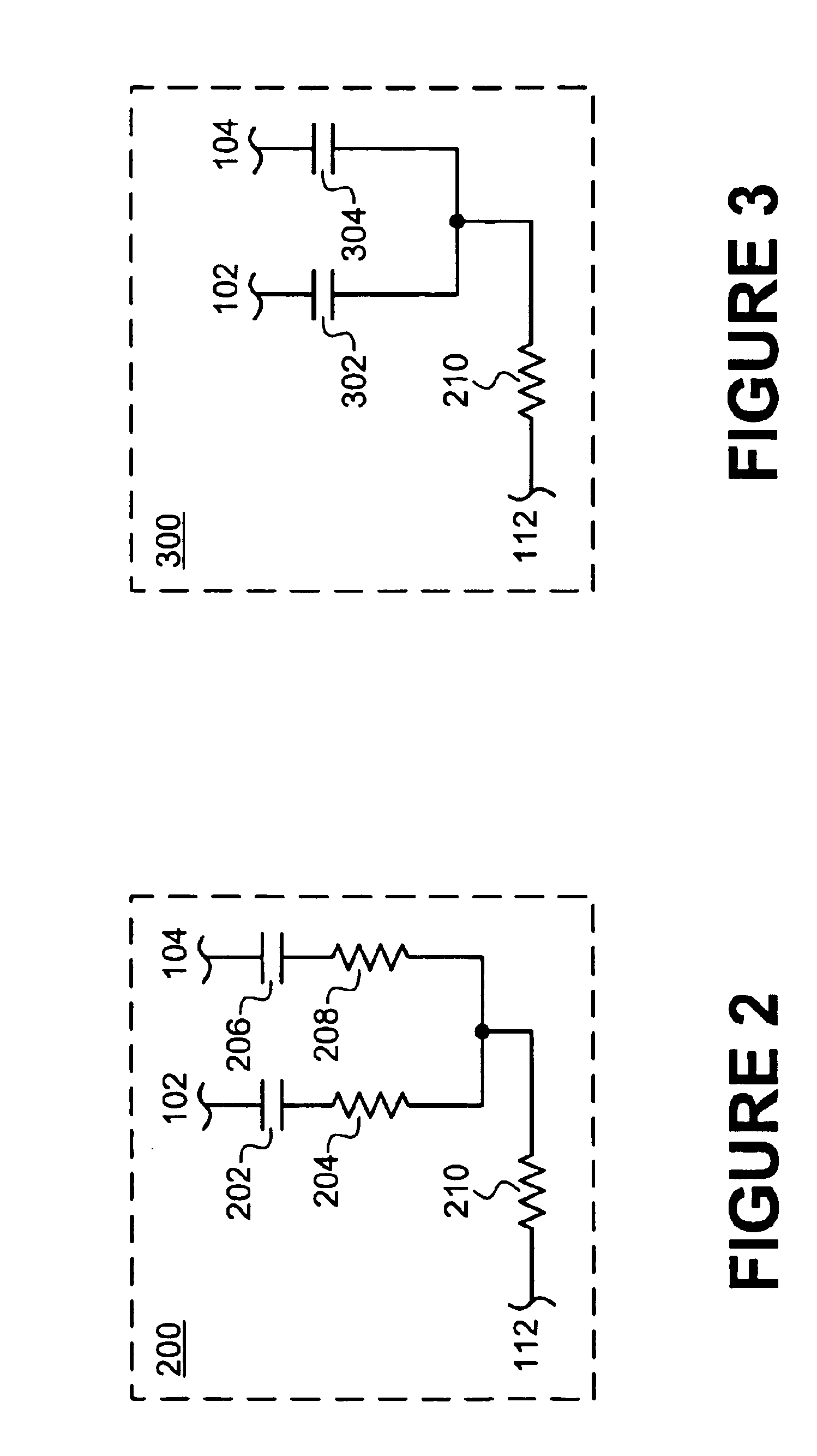
A CMOS varactor according to embodiments of the present invention is described herein. In the following description, numerous specific details, such as particular processes, materials, devices, and so forth, are presented to provide a thorough understanding of embodiments of the invention. One skilled in the relevant art will recognize, however, that the invention can be practiced without one or more of the specific details, or with other methods, components, etc. In other instances, well-known structures or operations are not shown or described in detail to avoid obscuring various embodiments of the invention.

Some parts of the description will be presented using terms such as transceiver, phase-locked loop, substrate, resistance, capacitance, jitter, and so forth. These terms are commonly employed by those skilled in the art to convey the substance of their work to others skilled in the art.

Other parts of the description will be presented in terms of operations performed by a compu...


PUM


Abstract

A differential varactor is physically defined in a CMOS process using a using the diffusion mask of a polycide gate rather than a P (+) mask, as is commonly used. The differential CMOS varactor may be used in a phase locked loop (PLL) of a voltage-controlled oscillator (VCO) to enable a transceiver to communicate at OC-3 / STM-1 data rates using SONET / SDH signaling formats.

Description

BACKGROUND OF THE INVENTION1. Field of the InventionThe present invention is related to integrated circuits and, in particular, to a variable capacitor in complementary metal oxide semiconductor (CMOS) process.2. Background InformationData access rates for Synchronous Optical Network (SONET) and Synchronous Digital Hierarchy (SDH) networks are steadily increasing as demand for web content move toward video-on-demand, streaming video, and audio, and teleconferencing applications. The current trend is to provide such high bandwidth access over coaxial cables and optical fibers has using SONET and SDH signaling formats. SONET specifies a set of transmission speeds (or data rates), which are multiples of the optical carrier level one (OC-1) channel data rate of 51.840 megabits per second (Mbps). For example, it is common to provide access at Optical Carrier level three / Synchronous Transfer Module 1 (OC-3) / (STM-1) rate, which is a data rate of 155.52 megabits per second (Mbps).To accompl...

Claims


Application Information

Patent Timeline
Patent Type & Authority Patents(United States)
IPC IPC(8): H01L29/66H01L29/93H01L27/08H03L7/099H03L7/08H04J3/06
CPCH01L27/0808H03L7/099H01L29/93H04J3/0685
Inventor ALTMANN, MICHAEL W.
Owner INTEL CORP
Why Eureka
Try Eureka