Detecting heat generating failures in unpassivated semiconductor devices

Inactive Publication Date: 2005-03-15
ADVANCED MICRO DEVICES INC
View PDF13 Cites 5 Cited by
  • Summary
  • Abstract
  • Description
  • Claims
  • Application Information

AI Technical Summary

Benefits of technology

The problems outlined above may at least in part be solved in some embodiments by applying a non-electrically conductive coating to an unpassivated su

Problems solved by technology

Semiconductor devices may experience failures, such as shorts, that arise when the semiconductor device is fabricated.
Similarly, components of the semiconductor devices may fail during testing

Method used


Image

  • Detecting heat generating failures in unpassivated semiconductor devices
  • Detecting heat generating failures in unpassivated semiconductor devices
  • Detecting heat generating failures in unpassivated semiconductor devices

Examples


Embodiment Construction

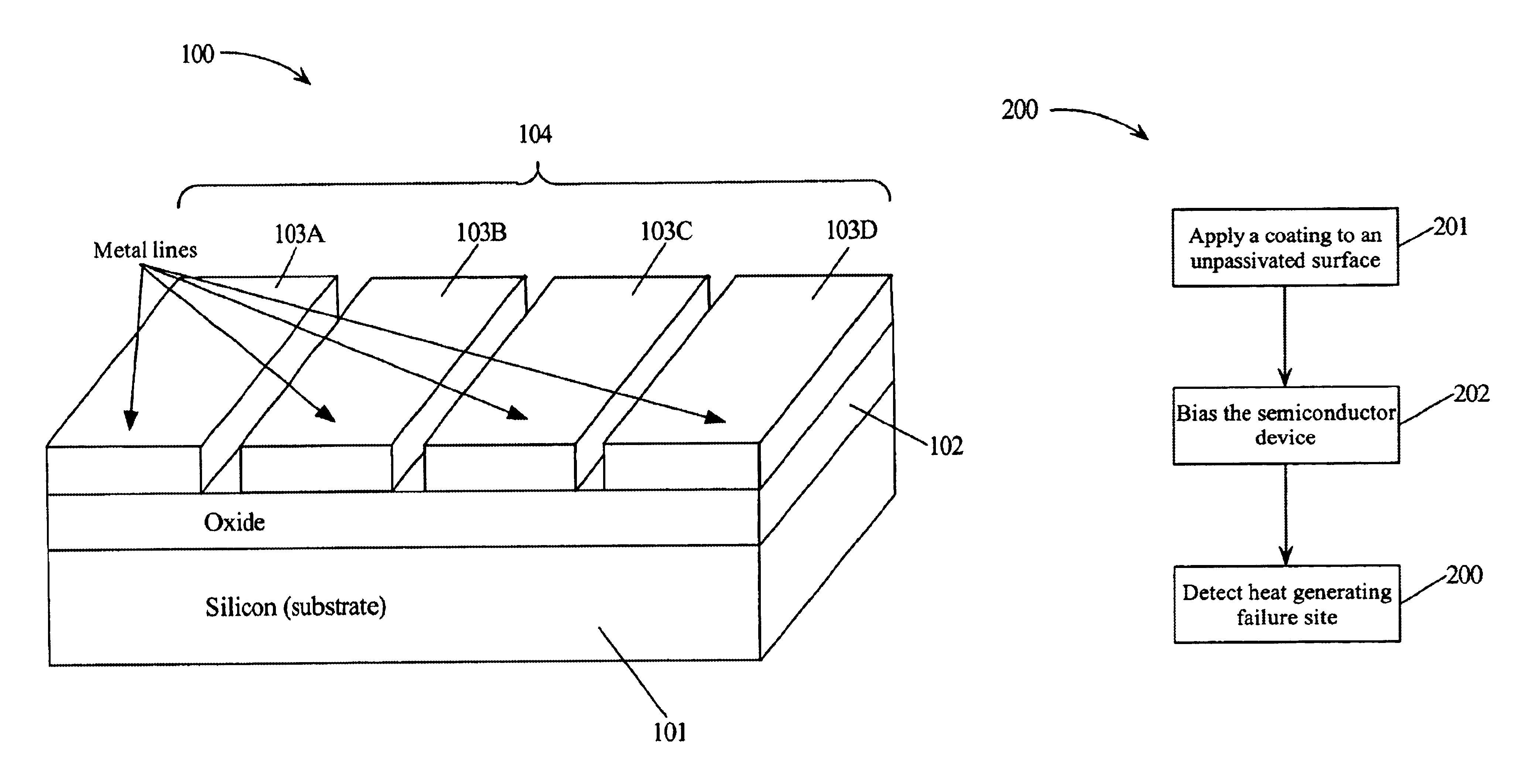
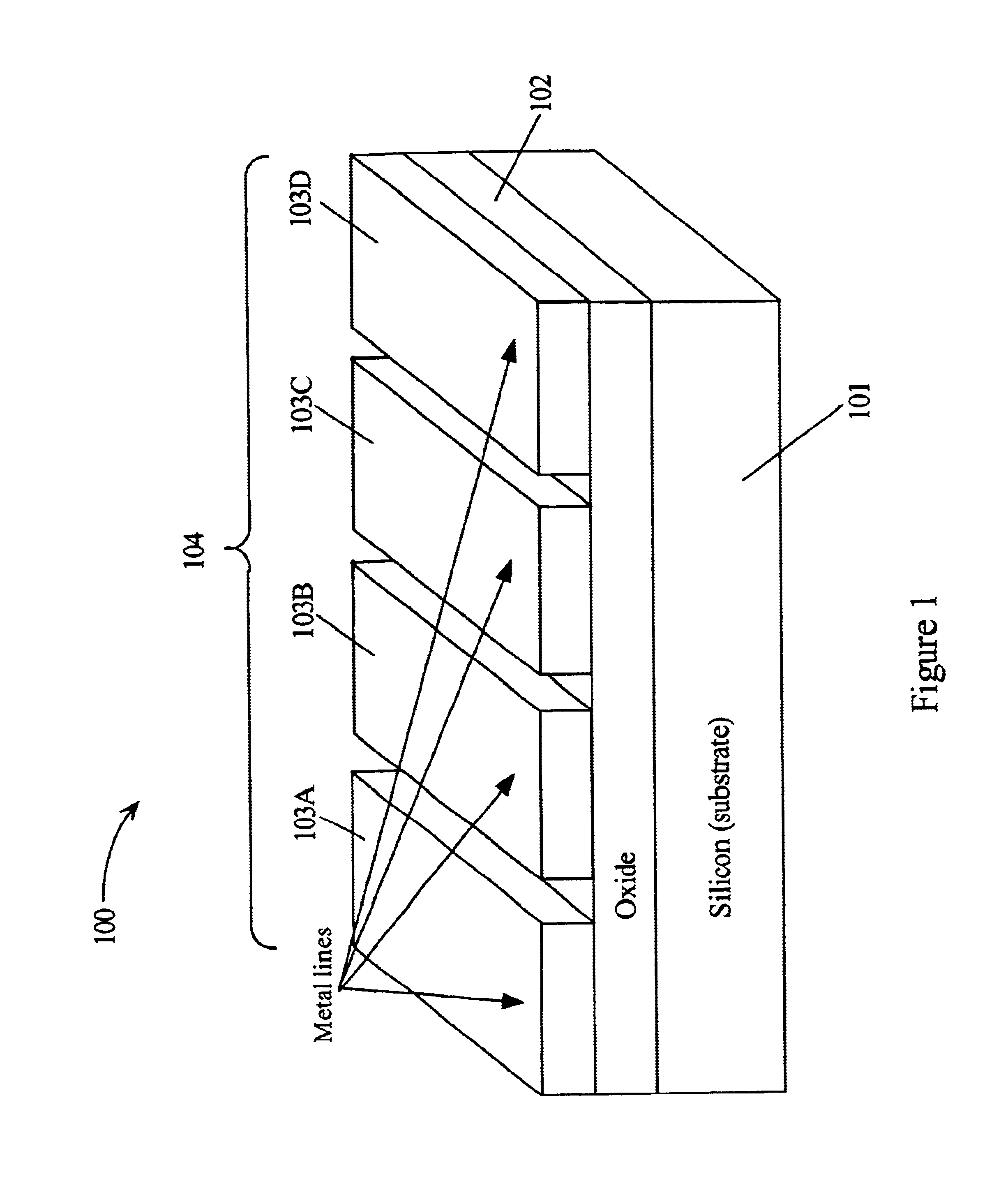
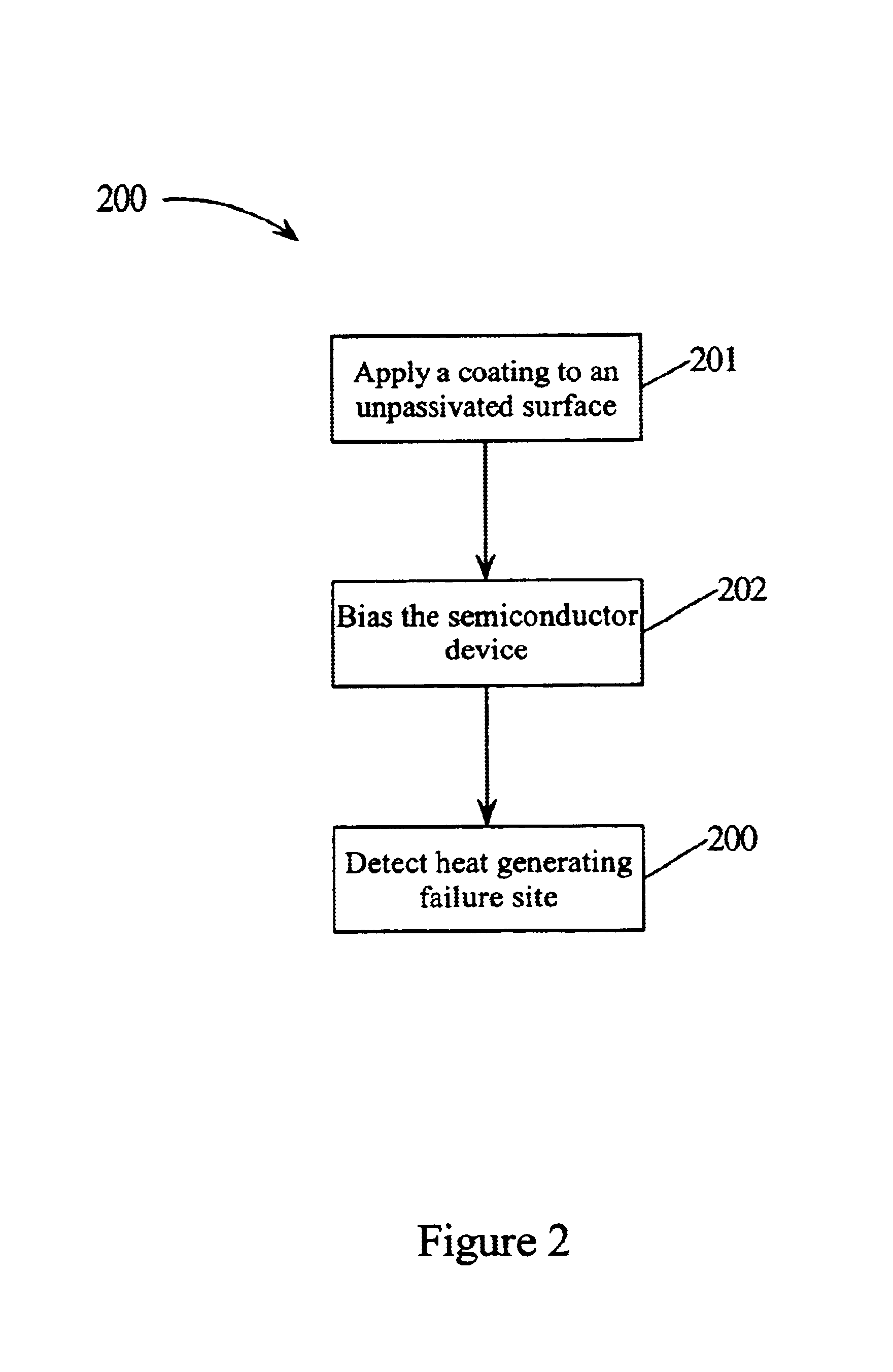
The present invention comprises a method and semiconductor device for detecting a heat generating failure in a semiconductor device having an unpassivated surface. A non-electrically conductive coating may be applied to the unpassivated surface of the semiconductor device where the coating may be capable of localizing heat generated by a heat-generating failure. The semiconductor device may be biased. Upon biasing the semiconductor device, a heat generating failure may be located by determining the location of the heat in the coating.

It is noted that the present invention relates to an improvement in failure analysis of semiconductor devices, particularly semiconductor devices having an unpassivated surface. The following description is presented to enable one of ordinary skill in the art to make and use the invention and is provided in the context of a patent application and its requirements. Various modifications to the disclosed embodiments will be readily apparent to those skill...


PUM


Abstract

A method and semiconductor device for detecting a heat generating failure in an unpassivated semiconductor device. The semiconductor device has an unpassivated surface and a heat generating failure, e.g., short circuit. A coating may be applied to the unpassivated surface of the semiconductor device. The coating may be non-electrically conducting and capable of localizing heat generated by the failure in a particular area. The semiconductor device may be biased. The failure may then be detected by detecting a location of the heat generated by the failure in the coating.

Description

TECHNICAL FIELDThe present invention relates to the field of semiconductor devices, and more particularly to detecting heat generating failures in an unpassivated semiconductor device (a semiconductor device with a surface not having a passivation layer) by placing a non-electrically conductive coating on the unpassivated surface.BACKGROUND INFORMATIONConventional semiconductor devices are fabricated with a large number of components. For example, a single semiconductor device may include a number of structures, such as gates, junctions, interconnects and contacts formed on an active area. The active area typically resides above a bulk silicon substrate of the semiconductor device. The structures formed may be desired to be electrically isolated. For example, although interconnects are designed to electrically connect certain portions of the semiconductor device, interconnects may be electrically isolated from the other interconnects. In another example, a floating gate may be elect...

Claims


Application Information

Patent Timeline
IPC IPC(8): G01N25/72G01N33/00
CPCG01N25/72G01N2033/0095
Inventor MAHANPOUR, MEHRDADCHOI, ALICE H.MASSOODI, MOHAMMADANG, BOON-YONG
Owner ADVANCED MICRO DEVICES INC
Why Eureka
Try Eureka