I/O buffer circuit

a buffer circuit and buffer technology, applied in the field of i/o (input/output buffers), can solve the problems of not implementing a function for increasing a voltage level, and cannot solve the problem and achieve the effect of high voltage input signal

Inactive Publication Date: 2005-03-29
LG ELECTRONICS INC
View PDF4 Cites 0 Cited by
  • Summary
  • Abstract
  • Description
  • Claims
  • Application Information

AI Technical Summary

Benefits of technology

[0025]It is another object of the present invention to provide a CM...

Problems solved by technology

However, the circuit shown in FIG. 2 can not solve the problem of the circuit in FIG.
1 and...

Method used


Image

  • I/O buffer circuit
  • I/O buffer circuit
  • I/O buffer circuit

Examples


Embodiment Construction

ide a further understanding of the invention and are incorporated in and constitute a part of this specification, illustrate embodiments of the invention and together with the description serve to explain the principles of the invention.

[0028]In the drawings:

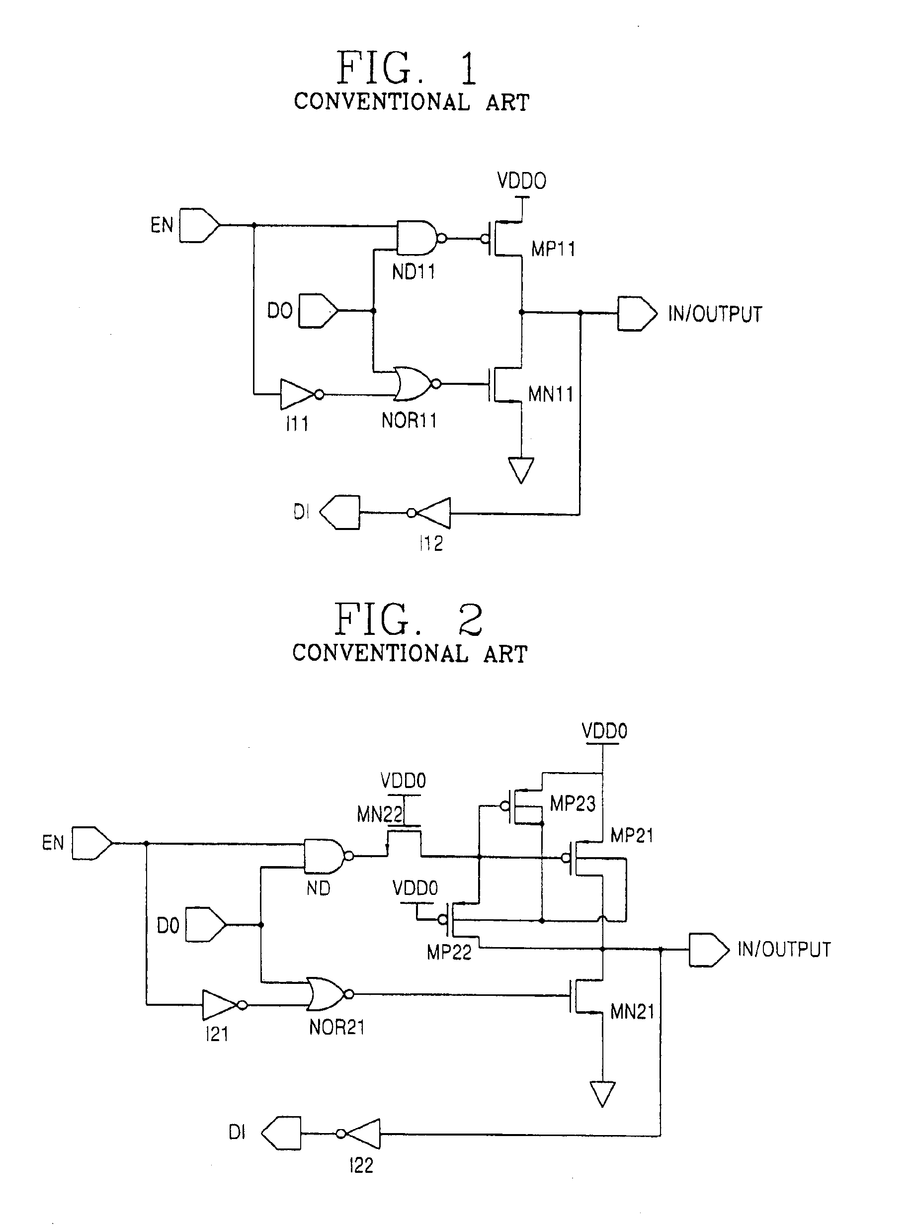
[0029]FIG. 1 is an exemplary view illustrating an I / O (input / output) buffer circuit in accordance with the conventional art;

[0030]FIG. 2 is an exemplary view illustrating another I / O buffer circuit in accordance with the conventional art; and

[0031]FIG. 3 is an exemplary view illustrating an I / O buffer circuit in accordance with the present invention.

DETAILED DESCRIPTION OF THE PREFERRED EMBODIMENT

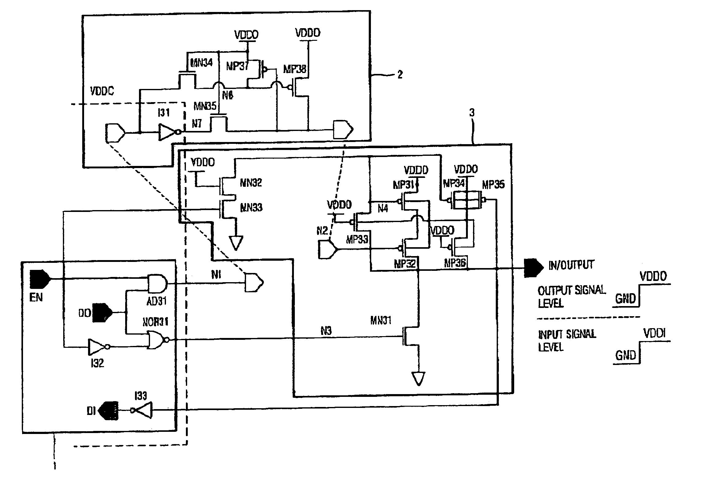
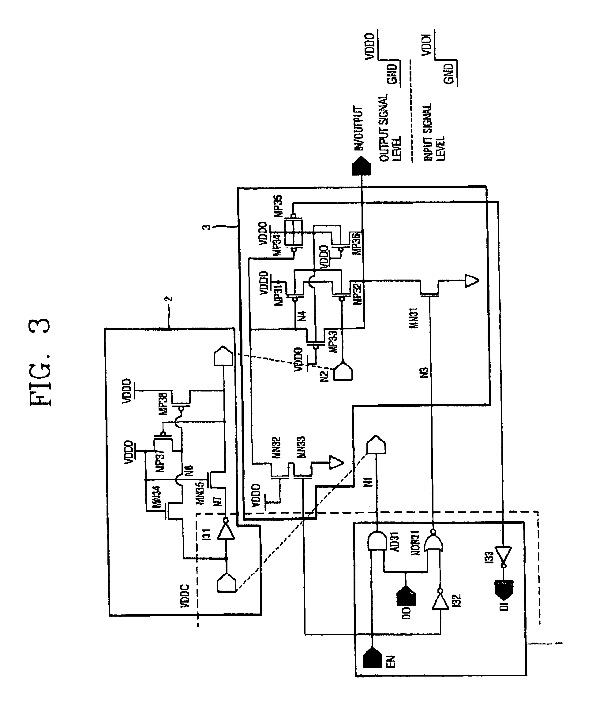
[0032]FIG. 3 is an exemplary view illustrating an I / O buffer circuit in accordance with the present invention.

[0033]As depicted in FIG. 3, an I / O buffer circuit in accordance with the present invention includes a logical controller 1 for generating an enable signal (EN) and data (DO) according to an internal core voltage (hereinafter, i...


PUM


Abstract

In an I/O buffer circuit for solving problems occurred due to I/O voltage level difference, the I/O buffer circuit includes a logical controller for generating an enable signal and data according to an internal core voltage (VDDC); a level converter for converting the internal core voltage (VDDC) into an output voltage level when the internal core voltage (VDDC), an input signal voltage (VDDI) and an output signal voltage (VDDO) are different; and a pull-up unit for permitting a voltage level in specific level order through the level converter when a power voltage level in a semiconductor chip and a voltage level of an input signal are different from each other.

Description

BACKGROUND OF THE INVENTION[0002]1. Field of the Invention[0003]The present invention relates to an I / O (input / output) buffer, and in particular to an I / O buffer circuit which is capable of permitting a voltage level in specific level order when voltage levels of input and output signals are different from each other.[0004]2. Description of the Prior Art[0005]With the development of semiconductor fabrication techniques, a size of a semiconductor device has been reduced, and accordingly a level of power voltage supplied to a semiconductor chip for operating an IC (integrated circuit) has been lowered gradually.[0006]On the other hand, input / output with the conventional semiconductor chip operated in a comparatively high power voltage level is requested continually. In particular, because a semiconductor chip using a core power voltage level and an output power voltage level differently has came into the market, it is required to solve problems caused by difference between an input si...

Claims


Application Information

Patent Timeline
IPC IPC(8): H03K19/003H03K19/0175
CPCH03K19/00315H03K19/0175
Inventor MOON, HONG-SHIK
Owner LG ELECTRONICS INC
Why Eureka
Try Eureka