
Offset drift compensating flat fielding method and camera used in millimeter wave imaging

a technology of offset drift and flat fielding, applied in the field of millimeter wave imaging, can solve the problems of not reaching the highest degree of flat fielding, and achieve the effects of effective account, good flat fielding, and uniform respons

Inactive Publication Date: 2005-04-12
MILLIVISION TECH
View PDF24 Cites 9 Cited by
  • Summary
  • Abstract
  • Description
  • Claims
  • Application Information

AI Technical Summary

Benefits of technology

The present invention involves normalizing or flat fielding the response characteristics of each radiometer channel or receiver channel in a millimeter wave imaging method and camera, in such a way as to more effectively account for factors which have not been adequately considered or recognized as important to deal with in previously known channel normalization or flat fielding techniques. As a consequence of the present invention, the channels have a more uniform response to a scene with a uniform brightness temperature, a characteristic referred to as flat fielding. Good flat fielding is a measure of enhancement of the image, because more contrast is obtained of points in the scene which emit different energies.

Problems solved by technology

By using the mean scene brightness temperature as the normalizing factor, previously known normalizing techniques could not fully account for individual differences in characteristics of the different channels and therefore could not achieve the highest degree of flat fielding.

Method used


Image

  • Offset drift compensating flat fielding method and camera used in millimeter wave imaging
  • Offset drift compensating flat fielding method and camera used in millimeter wave imaging
  • Offset drift compensating flat fielding method and camera used in millimeter wave imaging

Examples


Embodiment Construction

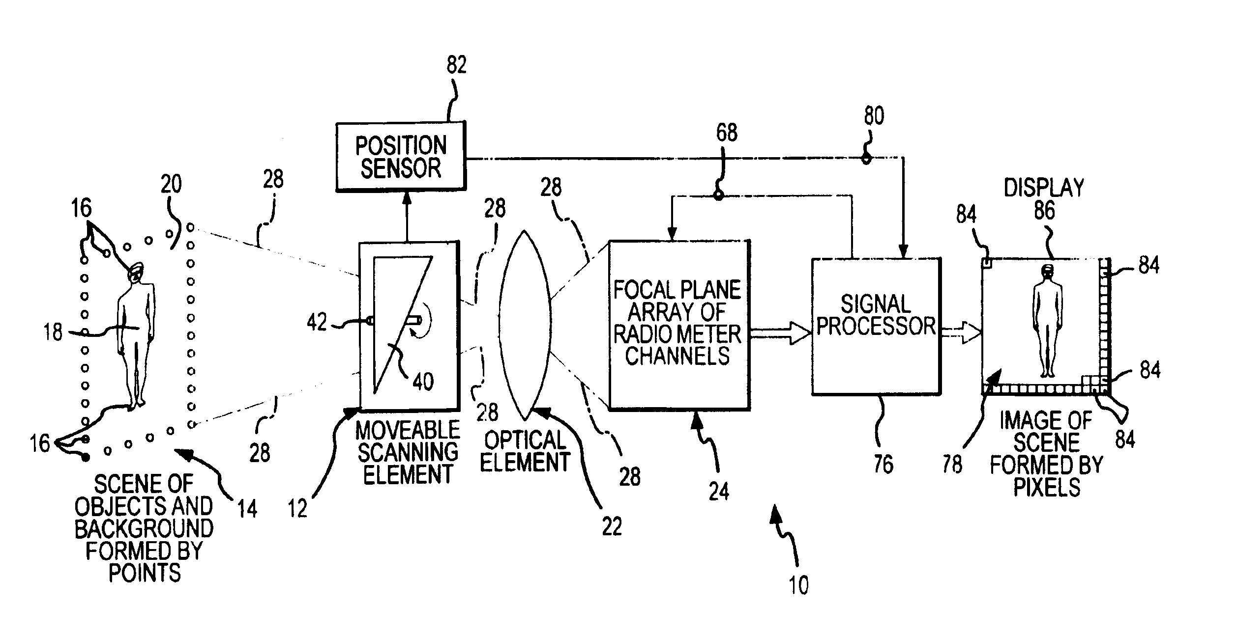
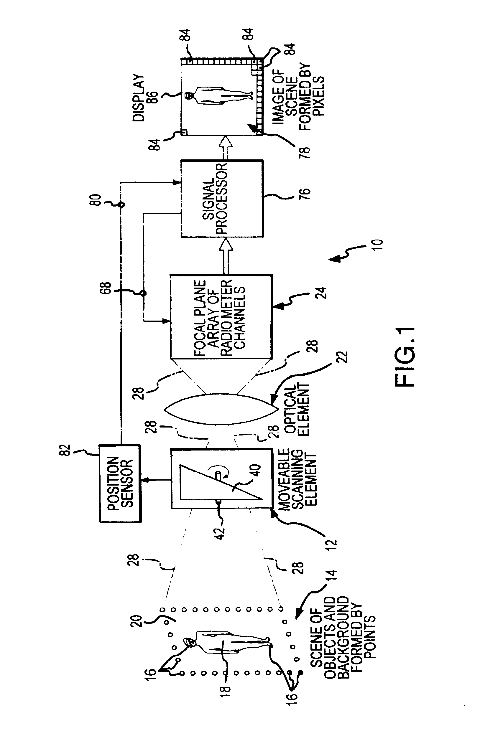
A camera 10, shown in FIG. 1, incorporates and operates in accordance with the various aspects of the present invention. The camera 10 includes a movable scanning element 12 which receives emitted and reflected radiation energy emanated from a scene 14. The scene 14 is formed by points 16, and each of the points 16 is either part of an object 18 within the scene 14 or part of a background 20 within the scene 14. The points 16 of the scene 14 emanate radiation energy with an intensity which is related to the brightness temperature of that point. The emanated radiation energy includes energy in a millimeter wavelength frequency band which is emitted and reflected from the objects 18 and the background 20.

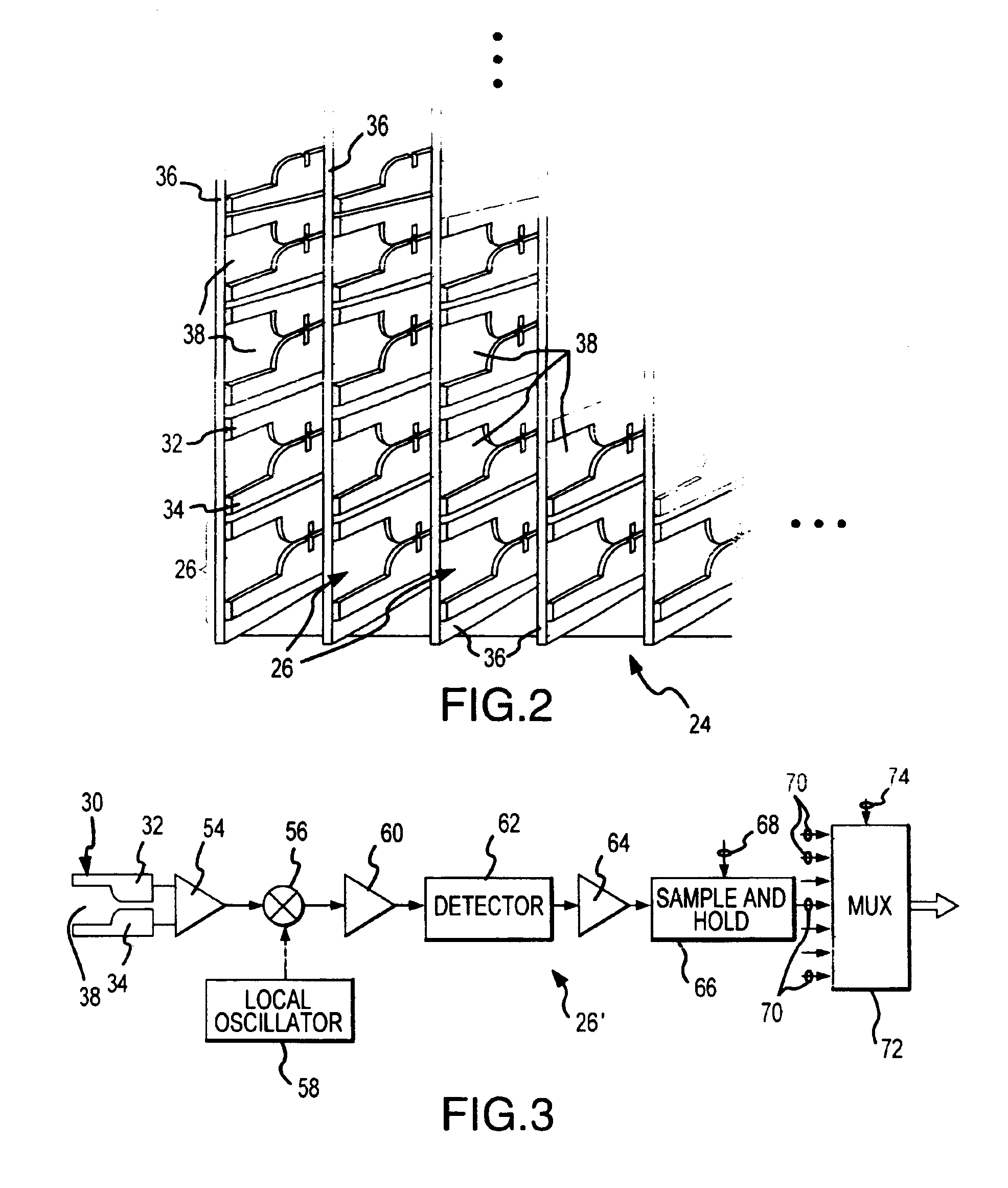
The movable scanning element 12 receives emanated energy from the scene 14, and directs or steers that energy through an optical element 22 to a focal plane array 24 of channels 26. Each channel 26 will typically be a radiometer channel when the camera 10 is used in passive imaging, a...


PUM


Abstract

Output value signals from radiometer or receiver channels are normalized to achieve a flat field response when creating a millimeter wave image. A normalizing factor is applied to the output value signals from each channel, and the normalizing factor accommodates drift in offset of the output value signals on a scan-by-scan basis. The normalizing factor is based on each channel observing a different mean scan brightness temperature from a portion of the scene than the mean brightness temperature of the entire scene. The normalizing factor is obtained by solving a system of simultaneous equations in which normalizing factors from all of the channels are related to one another, preferably by a consistency condition where the mean scan temperature of each channel is equal to an average of the intensities of those image pixels to which the output value signals from that channel contributes.

Description

FIELD OF THE INVENTIONThis invention generally relates to millimeter wave imaging. Millimeter wave imaging involves creating an image of a scene from millimeter wavelength energy signals emanating from the scene. More particularly, the present invention relates to a new and improved method and camera which compensates for drift in offset of output value signals supplied by each of a plurality of radiometer channels or receiver channels which receive and detect millimeter wavelength energy signals emanating from a scene. By compensating for the drift in offset, the individual and particular differences in the response of each channel are more accurately accounted for to improve the contrast and quality in an image composed by summing the output value signals from the channels.BACKGROUND OF THE INVENTIONMillimeter waves are electromagnetic radiation characterized by wavelengths in the range of from 1 to 10 millimeters and having corresponding frequencies in the range of 300 GHz to 30 ...

Claims


Application Information

Patent Timeline
Patent Type & Authority Patents(United States)
IPC IPC(8): G01S13/00G01S13/89H04N5/217H04N5/30
CPCH04N5/3651H04N5/30G01S13/887G01S13/89H04N25/671
Inventor VAIDYA, NITIN M.
Owner MILLIVISION TECH
Learn More