

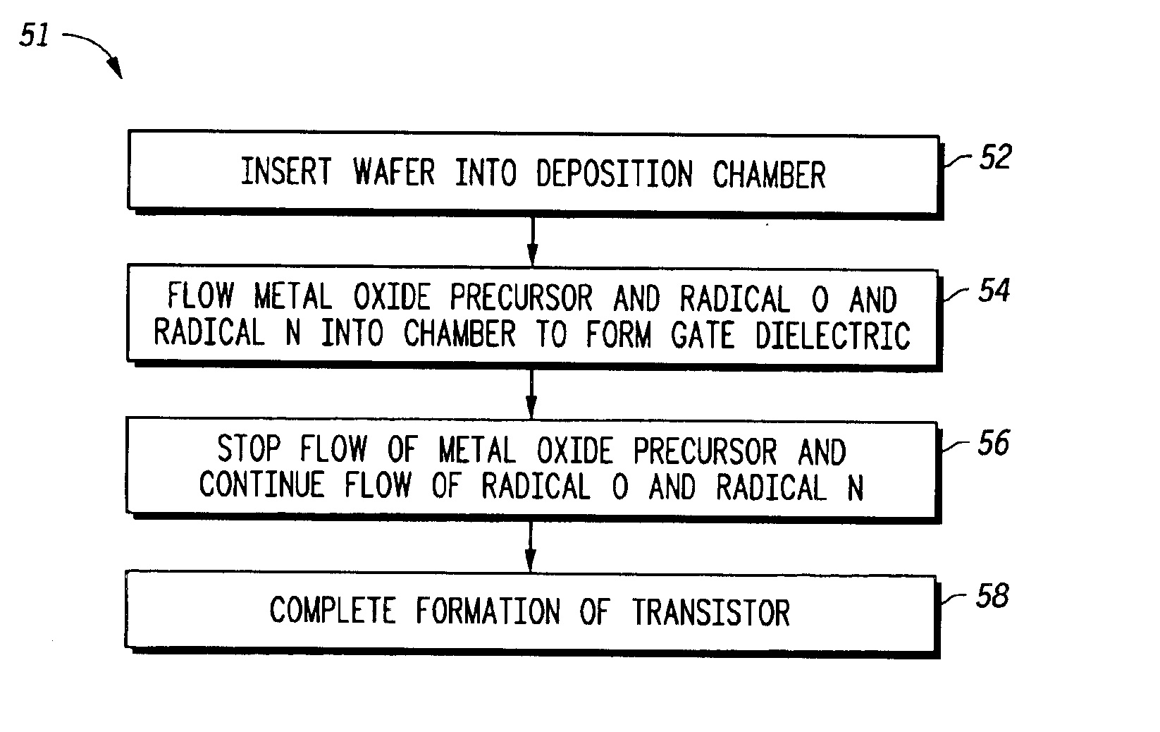
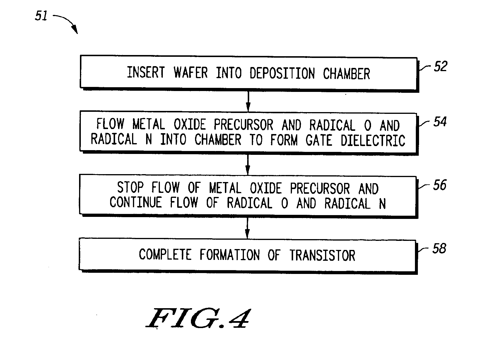
Radical oxidation and/or nitridation during metal oxide layer deposition process
- Summary
- Abstract
- Description
- Claims
- Application Information
AI Technical Summary
Problems solved by technology
Method used
Image

Examples
Embodiment Construction
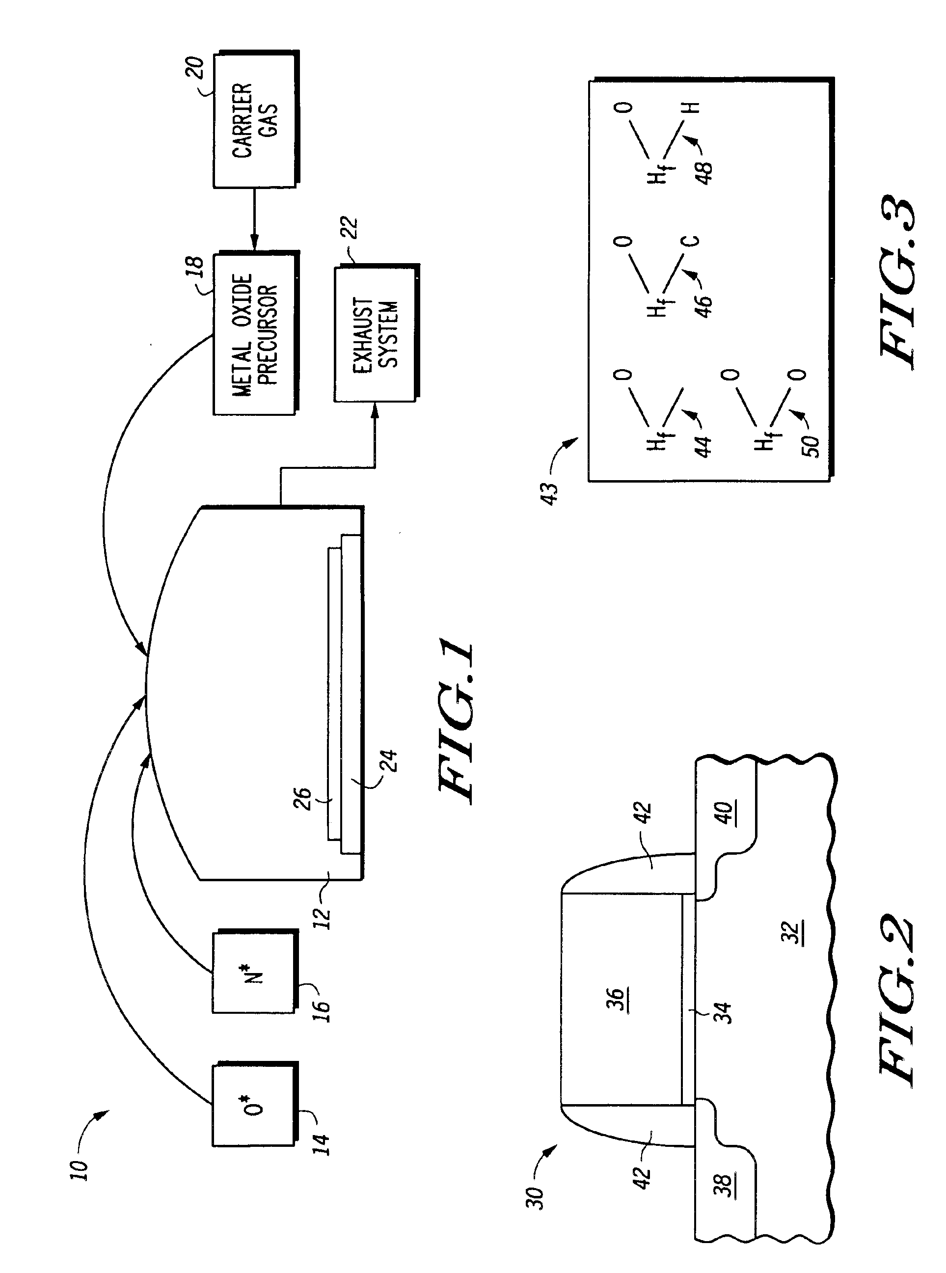
[0011]Illustrated in FIG. 1 is a deposition system 10 in accordance with the present invention and generally having a deposition chamber 12. A generator 14 for creating radical oxygen gas from an oxygen source (not shown) is coupled to a first inlet of the deposition chamber 12. A generator 16 for creating radical nitrogen gas from a nitrogen source (not shown) is coupled to a second inlet of the deposition chamber 12. A metal oxide precursor container 18 is coupled to a third inlet of the deposition chamber 12. The metal oxide precursor container 18 is connected to a container 20 for storing an inert carrier gas. An outlet of the deposition chamber 12 is coupled to an exhaust system 22. Within the deposition chamber 12 is a chuck 24 for holding a semiconductor wafer 26 containing predetermined integrated circuits. It should be readily understood that the deposition chamber 12 may be implemented to contain multiple wafers at the same time and that in such systems modification to the...
PUM
| Property | Measurement | Unit |
|---|---|---|
| Temperature | aaaaa | aaaaa |
| Thickness | aaaaa | aaaaa |
Abstract
Description
Claims
Application Information