Nonvolatile memory device with double serial/parallel communication interface

a technology of parallel communication and flash memory, which is applied in the field of flash memory devices with serial and parallel communication modes, can solve the problems of burdening the complexity of auxiliary circuits by double serial parallel functioning modes

Active Publication Date: 2005-05-10
MICRON TECH INC
View PDF8 Cites 16 Cited by
  • Summary
  • Abstract
  • Description
  • Claims
  • Application Information

AI Technical Summary

Benefits of technology

[0006]This and other objects, advantages and features in accordance with the present invention are provided by an architecture that exploits structures already present in a standard FLASH memory (such as certain internal buses, registers, etc.) and introduces a small number of additional structures. This permits the integration of a multi-mode memory in a device with a package and size substantially identical to those of a common FLASH memory for standard applications (parallel or pseudo parallel access mode) having a same capacity and with the same technology.

Problems solved by technology

Typically, these memory devices store a large volume of data that may remain unmodified or may be frequently modified.
An often required double serial-parallel functioning mode burdens the complexity of the auxiliary circuitry to be integrated in the memory device in addition to the functional circuitry of a standard FLASH memory.

Method used


Image

  • Nonvolatile memory device with double serial/parallel communication interface
  • Nonvolatile memory device with double serial/parallel communication interface
  • Nonvolatile memory device with double serial/parallel communication interface

Examples


Embodiment Construction

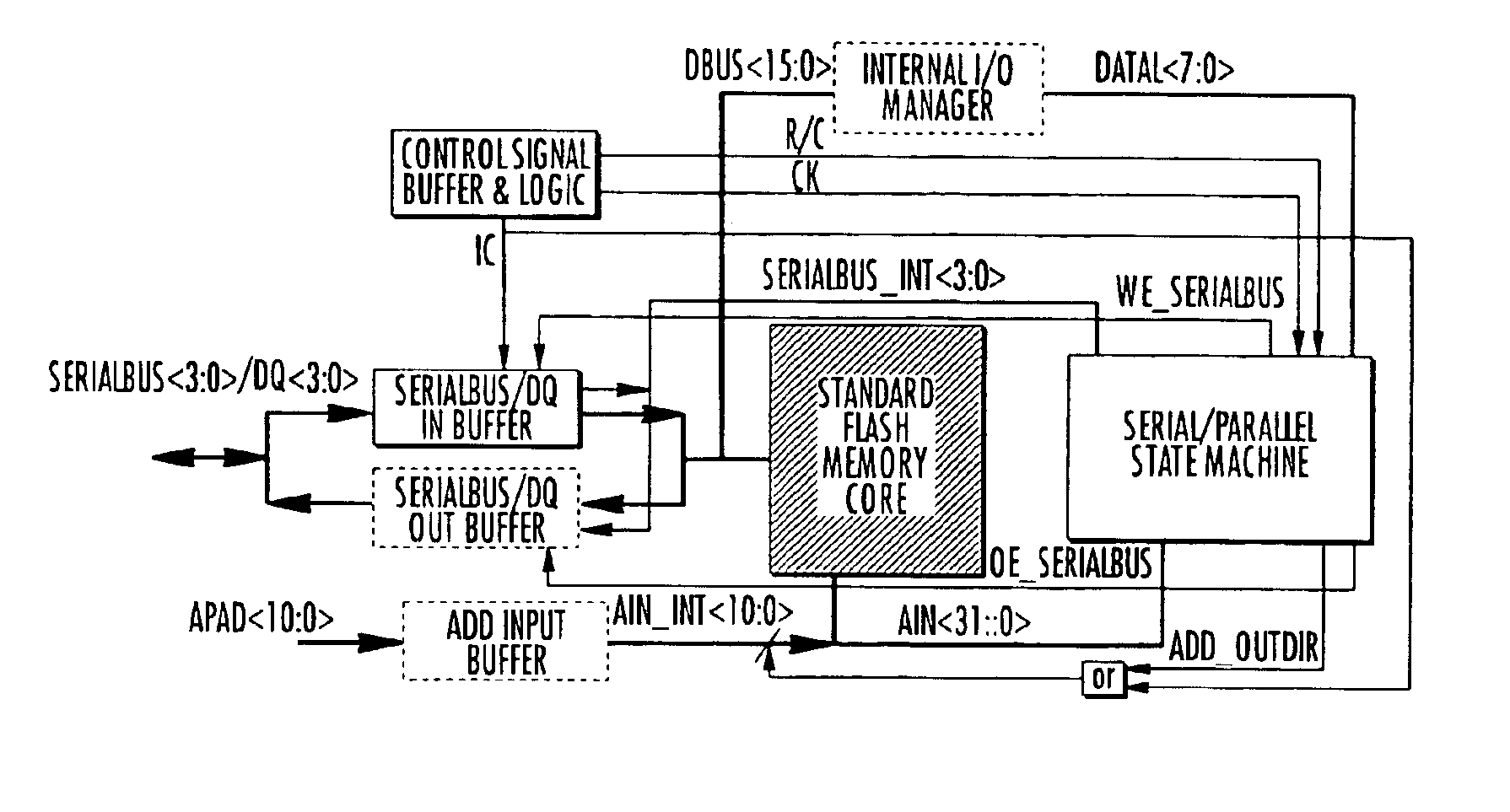
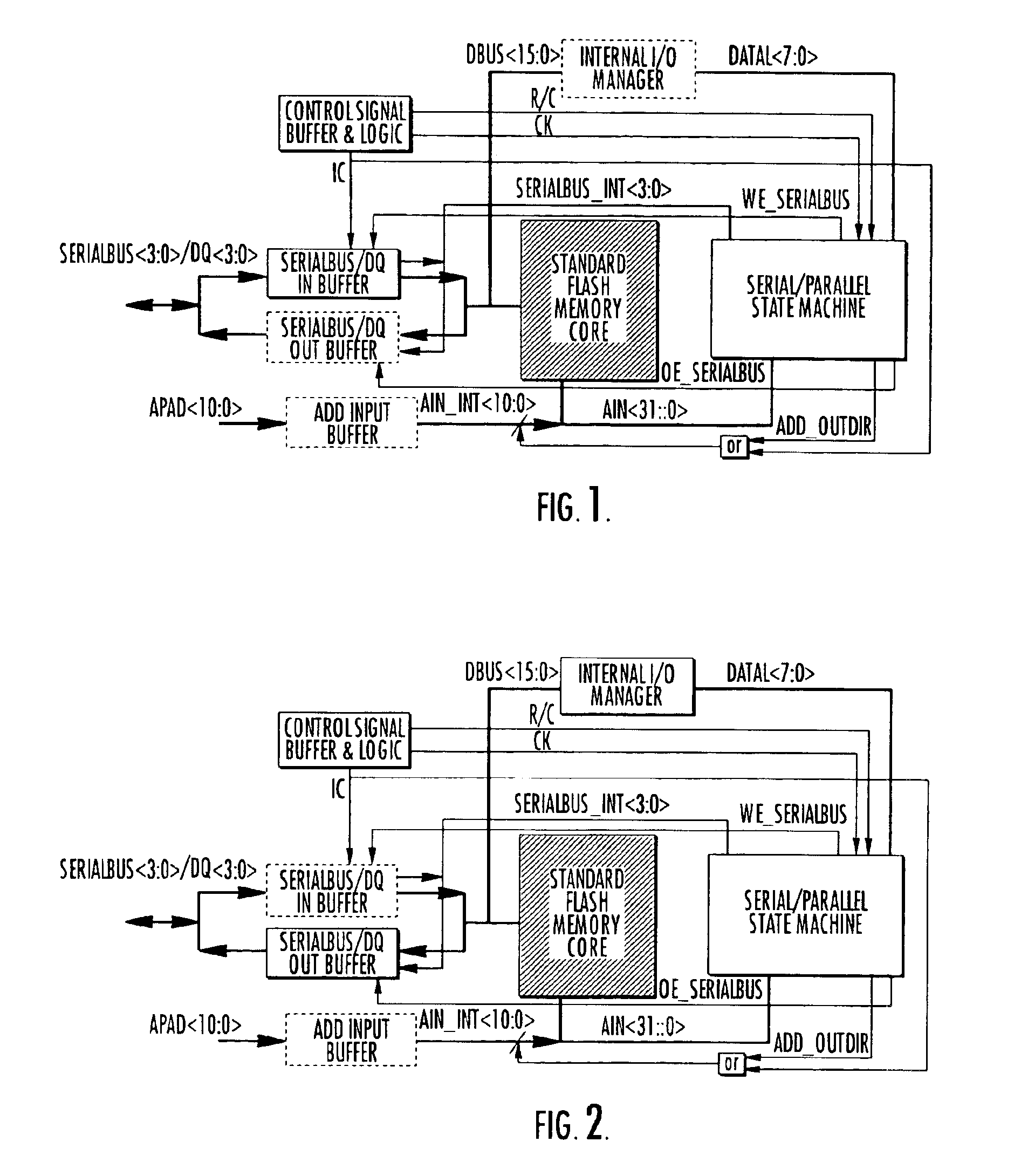
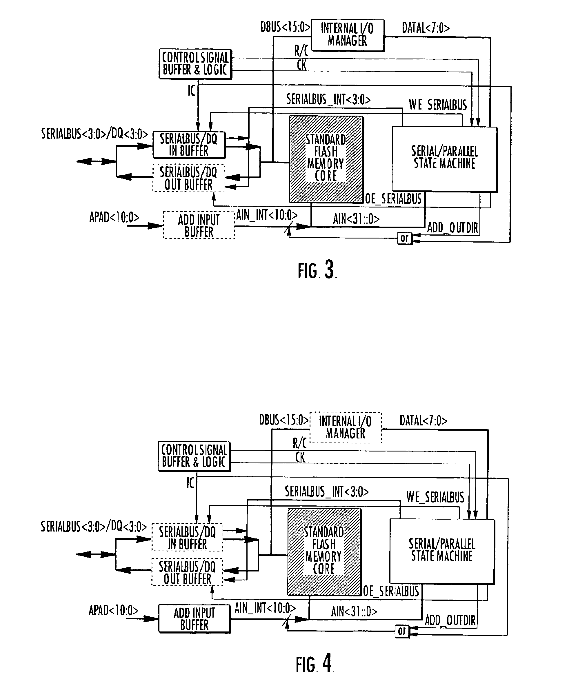
[0022]With reference to Figures from 1 to 6 which show a functional block diagram of the architecture of the present invention, the shaded blocks represent the circuit blocks that are normally present in a typical standard FLASH memory. In the figures, these blocks are represented external the block STANDARD FLASH MEMORY CORE simply to describe the manner in which they interconnect within the multi-mode (serial / parallel) interface architecture in accordance with the present invention.

[0023]The structural modifications to the functional blocks of a standard memory are limited substantially to the block SERIAL / PARALLEL STATE MACHINE. This block constitutes the multi-mode interface circuitry that implements the timing of the various phases of the memory for the different functioning modes. An additional internal bus DATAL7:0> is provided for transferring data present on the data bus DBUS15:0> of the standard architecture of the memory, through the input management circuit and the INTER...


PUM


Abstract

A nonvolatile memory device is operable in a serial mode and in a parallel mode. The architecture of the nonvolatile memory device is based upon the structure already present in a standard memory, but includes certain modifications. These modifications include the addition of a timing state machine for the various memory access phases (i.e., writing and reading data), and the addition of an internal bus and related logic circuits for disabling the internal address bus of the standard memory when the nonvolatile memory device operates in the serial mode.

Description

FIELD OF THE INVENTION[0001]The present invention relates in general to nonvolatile memory devices, and in particular, to a FLASH memory device with a double interface for serial and parallel communication modes.BACKGROUND OF THE INVENTION[0002]Large capacity nonvolatile memory devices which are commonly based on electrically erasable and programmable floating gate memory cells of the FLASH type are used in a number of applications. Typically, these memory devices store a large volume of data that may remain unmodified or may be frequently modified.[0003]In many applications that require a serial access mode for reading stored data, as well as for writing data in a memory array, the first or original factory programming of the memory device is commonly done in a parallel or pseudo-parallel mode. This programming is done by exploiting the “standard” parallel access mode structure of the memory device for speeding up the writing of a large volume of data in the memory before installin...

Claims


Application Information

Patent Timeline
Patent Type & Authority Patents(United States)
IPC IPC(8): G11C7/10G11C16/08G11C16/06G11C16/26
CPCG11C7/1075G11C16/08G11C2216/30G11C2207/107G11C16/26
Inventor POLIZZI, SALVATOREPOLI, SALVATOREPERRONI, MAURIZIO
Owner MICRON TECH INC
Why Eureka
Try Eureka