Tunneling floating gate APS pixel

a technology of floating gate and aps pixel, which is applied in the direction of diodes, radiation controlled devices, semiconductor devices, etc., can solve the problems of tunneling currents and problems in the design of aps pixel in 0.13 micron processing

Inactive Publication Date: 2005-05-24
UNITED MICROELECTRONICS CORP
View PDF7 Cites 40 Cited by
  • Summary
  • Abstract
  • Description
  • Claims
  • Application Information

AI Technical Summary

Benefits of technology

[0014]Designing an APS pixel in 0.13 micron processing presents problems due to high dark current and gate tunneling current. As dimensions shrink in CMOS process technology the gate oxides also become thinner. These thinner oxides, about 25 Angstroms, result in tunneling currents through the gate oxide. In many cases, such tunneling currents have been considered a problem in CMOS pixel design. This invention provides a pi

Problems solved by technology

Designing an APS pixel in 0.13 micron processing presents problems due to high dark current and gate tunn

Method used


Image

  • Tunneling floating gate APS pixel
  • Tunneling floating gate APS pixel
  • Tunneling floating gate APS pixel

Examples


Embodiment Construction

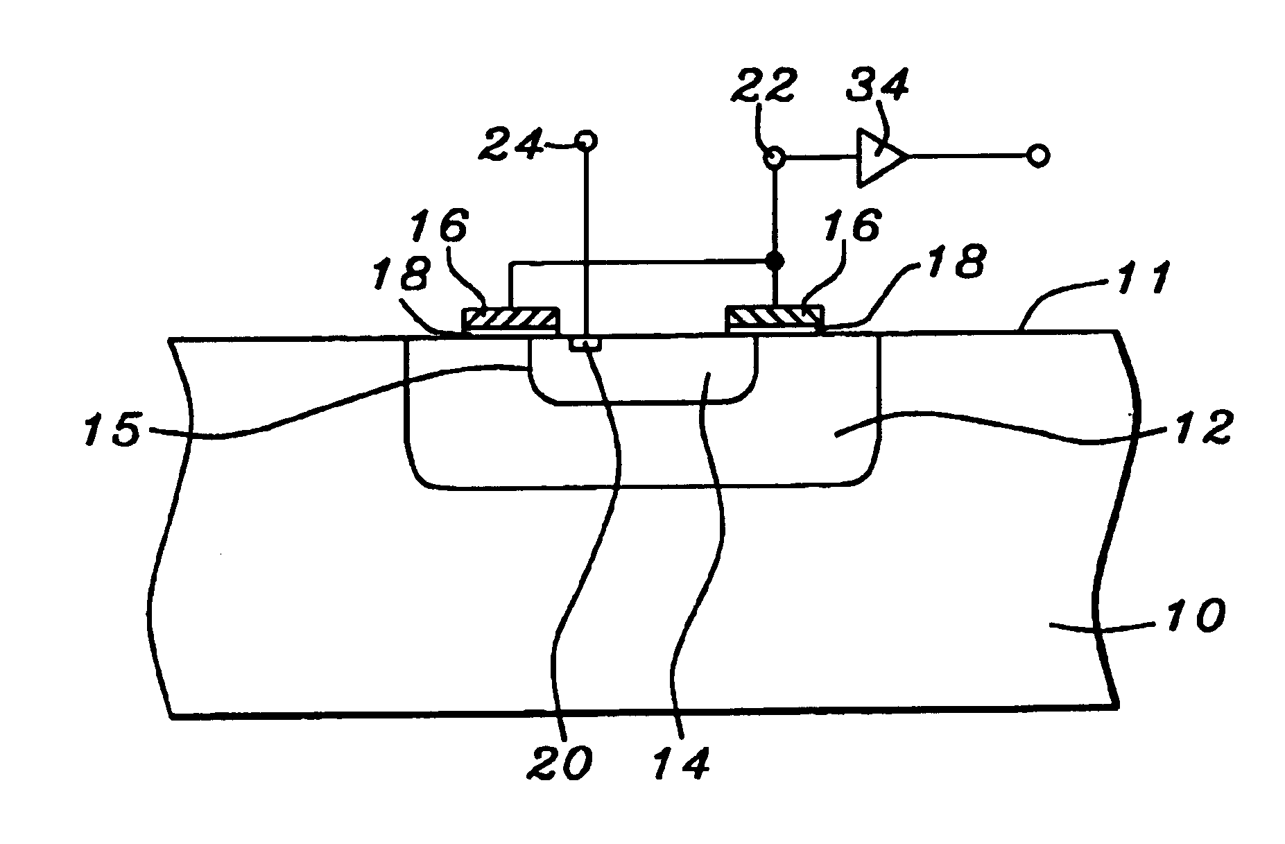
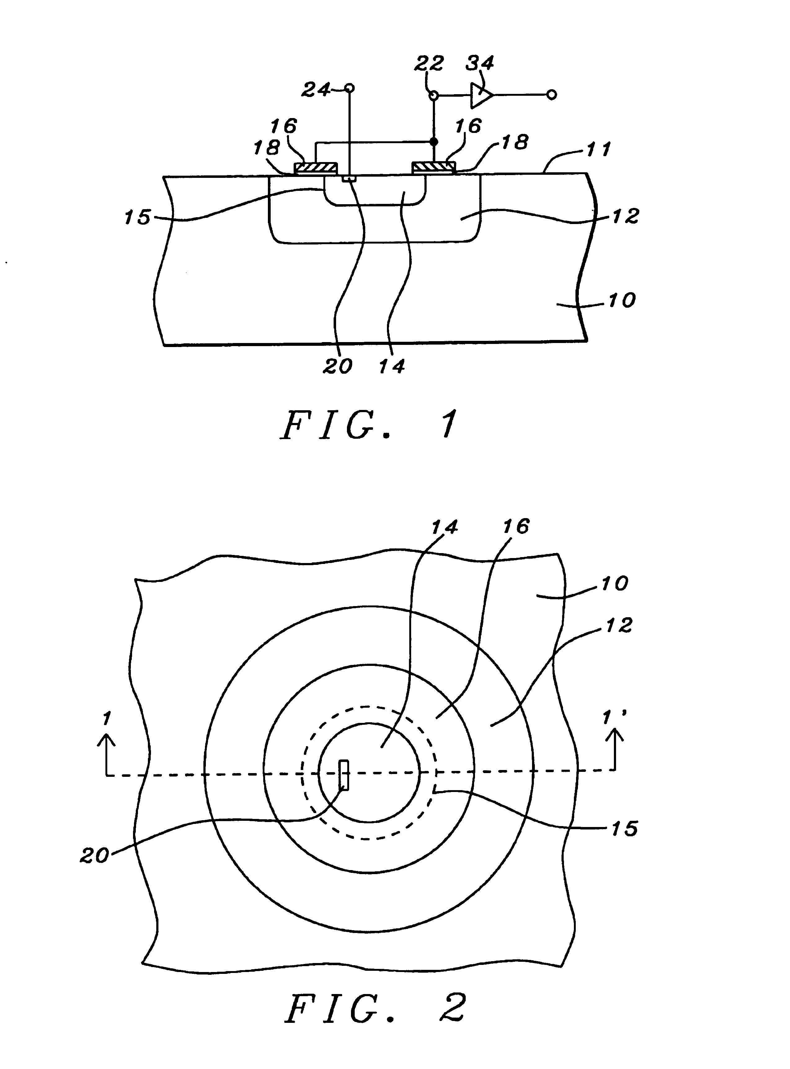
[0023]FIG. 1 shows a cross section view of an example of a floating gate pixel. An N well 12 is formed in a P type silicon substrate, usually a P type epitaxial silicon substrate. A P well 14 is formed in the N well 12. The only contact to the pixel structure is in the P well 14 and is shown as a single P+ type contact 20 in FIG. 1. This P+ type contact 20 allows the pixel to be reset and serves as a source / drain region. A gate oxide 18 is formed on the substrate and a gate electrode 16 is formed on the gate oxide 18. Although two sections of the gate electrode 16 are shown in FIG. 1 the two sections are part of a single gate electrode. The gate electrode has a closed shape such as a donut shape and is connected to an output terminal 22. The gate oxide 18 and the gate electrode 16 are directly over part of the P well 14, part of the N well 12, and the intersection of the PN junction 15 between the P well 14 and the N well 12 and the top surface 11 of the pixel. Altematively the gate...


PUM


Abstract

A floating gate pixel is described which is formed by forming an N well in a P type silicon substrate. A P well is formed in the N well A gate is formed over a thin gate oxide, about 25 Angstroms thickness, such that the gate is directly over part of the P well and part of the N well. A P+ contact in the P well allows connection to a reset voltage source, usually through a reset transistor, to reset the pixel. The pixel is reset by setting the potential between the P well and the substrate, which is usually held at ground potential. When the pixel is reset tunneling current through the thin gate oxide sets the voltage of the floating gate. During the charge integration cycle an input signal to the pixel, such as a light signal, changes the potential of the pixel. After the charge integration cycle the tunneling current through the gate oxide changes the potential of the floating gate by an amount related to the input signal to the pixel. The potential of the floating gate can then be read out to determine the input signal to the pixel. The pixel can also be embodied using a P well formed in an N type substrate, an N well formed in the P well, and an N+ contact formed in the N well.

Description

[0001]This Patent Application claims priority to the following U.S. Provisional Patent Application, herein incorporated by reference:[0002]Provisional Application No. 60 / 450,091 filed Jan. 26, 2003.BACKGROUND OF THE INVENTION[0003](1) Field of the Invention[0004]This invention relates to a tunneling floating gate APS pixel and more particularly to advantageously using tunneling current in a thin oxide in pixel operation.[0005](2) Description of The Related Art[0006]In a CMOS APS pixel structure having very thin gate oxides tunneling currents will occur through the gate oxide. These tunneling currents must be taken into account in the operation of these pixels.[0007]U.S. Pat. No. 6,008,486. to Stam et al. describes a method for increasing effective integration time of an optical sensor. In some of the embodiments a floating diffusion is used in the operation of the pixel, however in one embodiment the floating diffusion is replaced by a floating gate.[0008]U.S. Pat. No. 6,501,109 B1 ...

Claims


Application Information

Patent Timeline
IPC IPC(8): H01L29/66H01L29/788H01L31/06H01L27/146H01L31/112
CPCH01L27/14603H01L31/112H01L27/14643
Inventor DOSLUOGLU, TANER
Owner UNITED MICROELECTRONICS CORP
Why Eureka
Try Eureka