Semiconductor device having divided active regions with comb-teeth electrodes thereon

a technology of active regions and semiconductor devices, which is applied in the direction of semiconductor devices, semiconductor/solid-state device details, electrical apparatus, etc., can solve the problems of increasing the device characteristics are degraded, and the distance between the pad and the transistor increases

Inactive Publication Date: 2005-05-31
FUJITSU QUANTUM DEVICES LTD
View PDF9 Cites 35 Cited by
  • Summary
  • Abstract
  • Description
  • Claims
  • Application Information

AI Technical Summary

Benefits of technology

[0005]An object of the present invention is to provide a semiconductor device for power amplification attaining a desired power amplification without degradation of the above-mentioned device characteristics.

Problems solved by technology

However, the increase of the channel width needs the corresponding increase of the gate finger 1, a drain finger 2 and a source finger 3 lengthwise, which results in degradation of device characteristics due to increase of inner resistance of the respective fingers.
To avoid this problem, it could be possible to increase the numbers of parallel transistors maintaining the channel width unchanged, by which the power amplification would be increased without increase of the inner resistance, but the increase of the numbers of parallel transistors by simple increase of the active region in the channel-length direction leads to increase in length of the respective bars, which results in an adverse effect that difference in distance from a pad to each of transistors increases because the distance depends upon relative disposition of the respective transistor to the pad.
For this reason, the larger difference in the distance incurs more difficulty in a high-speed parallel operation.

Method used


Image

  • Semiconductor device having divided active regions with comb-teeth electrodes thereon
  • Semiconductor device having divided active regions with comb-teeth electrodes thereon
  • Semiconductor device having divided active regions with comb-teeth electrodes thereon

Examples


embodiment 1

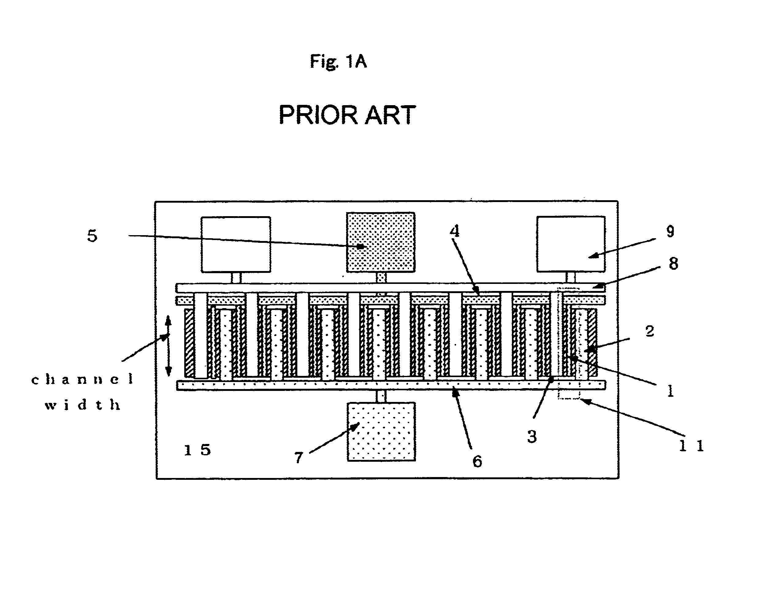
[0027]FIG. 2 a top view of a power FET for the first embodiment according to the present invention.

[0028]As shown in FIG. 2, a pair of parallel rectangular-shaped active regions 10 are formed on the front surface of the substrate 15. An array of parallel transistors are formed in each of the active regions. Each of the gate, drain and source fingers is laid out in tandem in the direction of finger-length on the pair of the active regions. Since this configuration prevents each of the gate, drain and source bars from increasing in length, and suppresses increase of difference in distance from each of the pads to all of the corresponding fingers, depending upon disposition of the transistors in one of the active regions, each of the gate, drain and source bars can supply an identical electric potential to all of the corresponding fingers essentially at the same time. Each of the bars is extended in perpendicular to the corresponding fingers, and each of the bars and the corresponding ...

embodiment 2

[0029]FIG. 3 is a top view of a power FET for the second embodiment according to the present invention.

[0030]As shown in FIG. 3, a transistor area can be saved by laying out the drain bar and source bar on the drain fingers and source fingers, respectively, in which an electric connection between the bar and fingers is made by a via-hole. Although only a pair of gate fingers arranged in tandem are shown by the embodiments in FIGS. 2 and 3, a triple or a multiple more than a pair arrangement is within the scope of the present invention.

embodiment 3

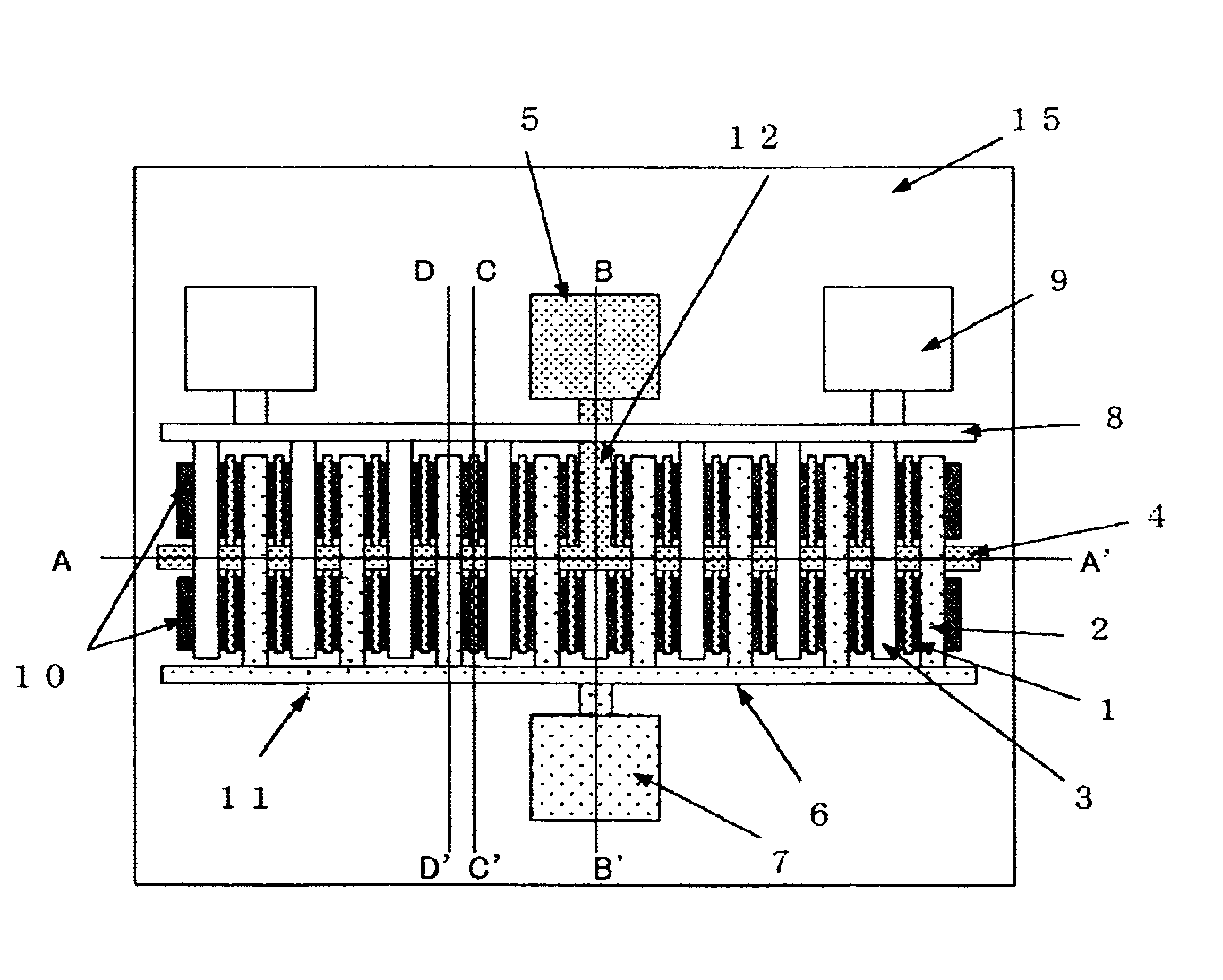
[0031]FIG. 4 is a top view of a power FET for the third embodiment according to the present invention, more specifically a 3-dimensional monolithic microwave integrated circuit (MMIC).

[0032]FIGS. 5-8 are cross-sectional views of the power FET along A-A′, B-B′, C-C′ and D-D′ lines shown in FIG. 4, respectively.

[0033]As shown in FIG. 4, two rectangular-shaped active regions 10 are arranged in parallel to each other on a semi-insulating GaAs substrate 15, and each of the gate fingers 1 is formed on the corresponding active region 10 connected to each other by a common gate bar 4. Drain fingers 2 and source fingers 3 cross over the gate bar 4 with an insulating layer 14 therebetween as shown in FIG. 5. The gate bar 4 and a gate pad 5 are connected by an upper conducting layer 12 formed on the insulating layer 14 as shown in FIG. 6. Furthermore, the upper conducting layer 12 is overlapped with one of the source fingers with the insulating layer therebetween. A portion of the gate bars 4 ...


PUM


Abstract

A high-frequency semiconductor device for power amplification has a comb-teeth electrode on each of active regions formed on the front surface of the semiconductor substrate. One aspect of the present invention, there is provided a monolithic microwave integrated circuit (MMIC) having a plurality of rectangular-shaped active regions arranged side by side on the front surface of the semiconductor substrate, each of the active regions having interdigited gate, drain and source electrodes thereon which are connected to the respective pads by multilayer interconnection technique. Additionally, the source potential is fed from the back surface of the substrate through a metal plugged via-hole.

Description

BACKGROUND OF THE INVENTION[0001]1. Field of the Invention[0002]The present invention relates to a semiconductor device for power amplification, and more particularly, to arrangement of active regions and electrodes for power transistors.[0003]2. Description of the Related Art[0004]A power semiconductor device using compound semiconductor materials for various applications such as local ground stations of mobile telephone network requires characteristics of high-speed operation and low power consumption. FIGS. 1A and 1B are a top view and a cross-sectional view in a unit transistor region of a conventional power semiconductor device, respectively. Hereinafter, the same numerals are designated to the same elements in all figures. As shown in FIGS. 1A and 1B, a conventional field effect transistor for power amplification (or a power FET) comprises a parallel array of unit transistors 11 disposed in an active region 10 on a compound semiconductor substrate 15 such as gallium-arsenide (...

Claims


Application Information

Patent Timeline
Patent Type & Authority Patents(United States)
IPC IPC(8): H01L29/06H01L29/423H01L29/66H01L29/02H01L29/80H01L29/40H01L21/338H01L29/812
CPCH01L29/0692H01L29/802H01L29/42316
Inventor AOKI, YOSHIOMIMINO, YUTAKABABA, OSAMUGOTOH, MUNEHARU
Owner FUJITSU QUANTUM DEVICES LTD
Why Eureka
Try Eureka