Electrostatic discharge (ESD) protection structure with symmetrical positive and negative ESD protection

a protection structure and electrostatic discharge technology, applied in the direction of semiconductor devices, electrical equipment, transistors, etc., can solve the problem that most conventional esd protection structures can only pro

Active Publication Date: 2005-06-14
NAT SEMICON CORP
View PDF5 Cites 25 Cited by
  • Summary
  • Abstract
  • Description
  • Claims
  • Application Information

AI Technical Summary

Benefits of technology

[0011]In accordance with one embodiment of the presently claimed invention, an electrostatic discharge (ESD) protection structure with a diac includes one or more reference electrodes, a circuit electrode, a semiconductor material, semiconductor regions and semiconductor wells. The semiconductor material is of a first conductivity type and in electrical communication with one or more of the one or more reference electrodes. A first semiconductor region of the first conductivity type is disposed on the semiconductor material and in electrical communication with at least one of the one or more reference electrodes. A second semiconductor region of a second conductivity type is disposed on the semiconductor material proximate the first semiconductor region and in electrical communication with the at least one of the one or more reference electrodes. A first semiconductor well of the second conductivity type is disposed in the semiconductor material. A second semiconductor well of the first conductivity type is disposed in the first semiconductor well. A third semiconductor region of the first conductivity type is disposed on the second semiconductor well and in electrical communication with the circuit electrode. A fourth semiconductor region of the second conductivity type is disposed on the second semiconductor well and in electrical communication with the circuit electrode.
[0012]In accordance with another embodiment of the presently claimed invention, an electrostatic discharge (ESD) protection structure with a diac includes one or more reference electrodes, a circuit electrode, a semiconductor material, semiconductor regions and semiconductor wells. The semiconductor material is of a first conductivity type and in electrical communication with one or more of the one or more reference electrodes. A first semiconductor region of the first conductivity type is disposed on the semiconductor material and in electrical communication with at least one of the one or more reference electrodes. A second semiconductor region of the second conductivity type is disposed on the semiconductor material proximate the first semiconductor region and in electrical communication with the at leas

Problems solved by technology

Most conventional ESD protection structures can on

Method used


Image

  • Electrostatic discharge (ESD) protection structure with symmetrical positive and negative ESD protection
  • Electrostatic discharge (ESD) protection structure with symmetrical positive and negative ESD protection
  • Electrostatic discharge (ESD) protection structure with symmetrical positive and negative ESD protection

Examples


Embodiment Construction

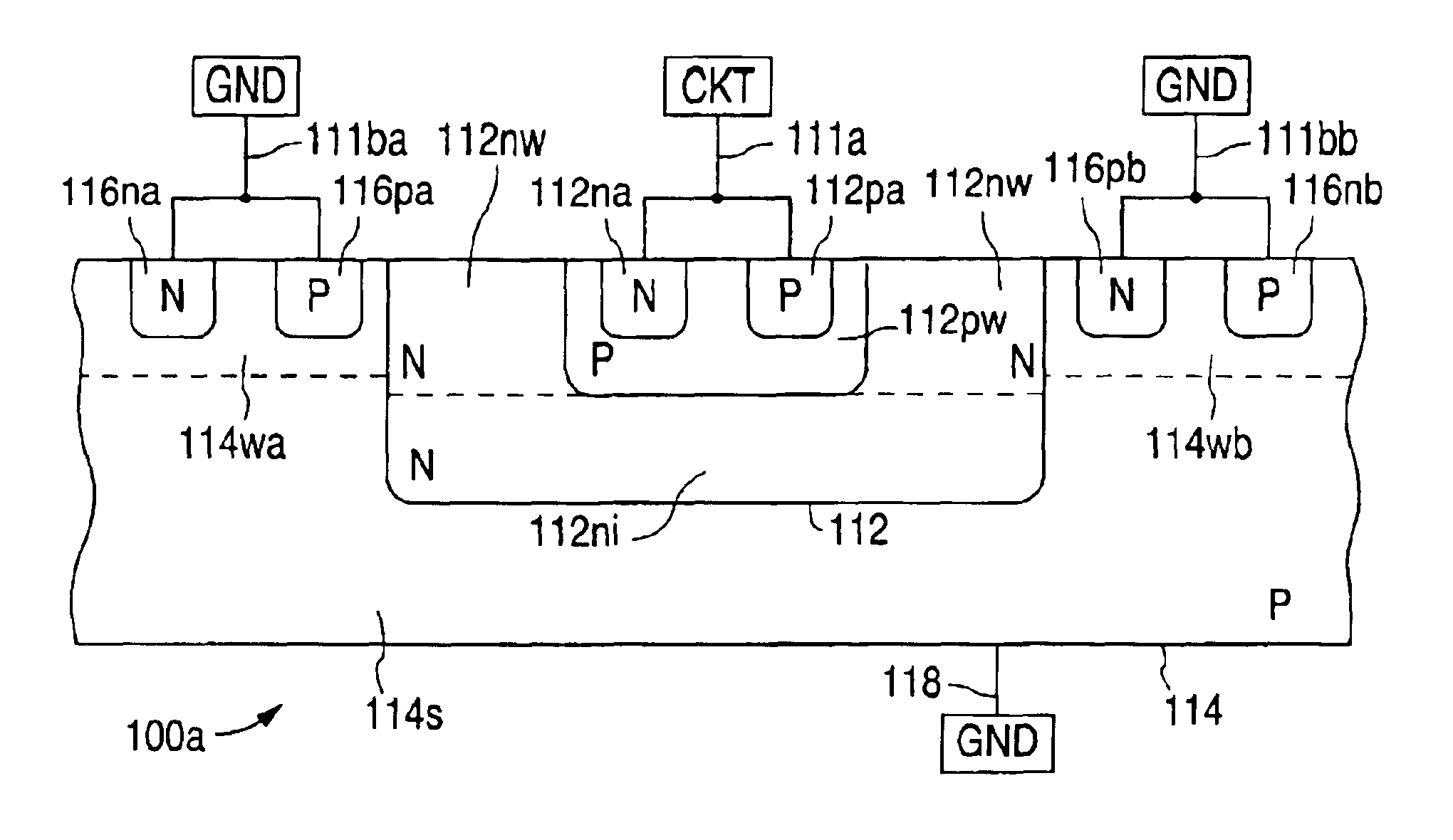
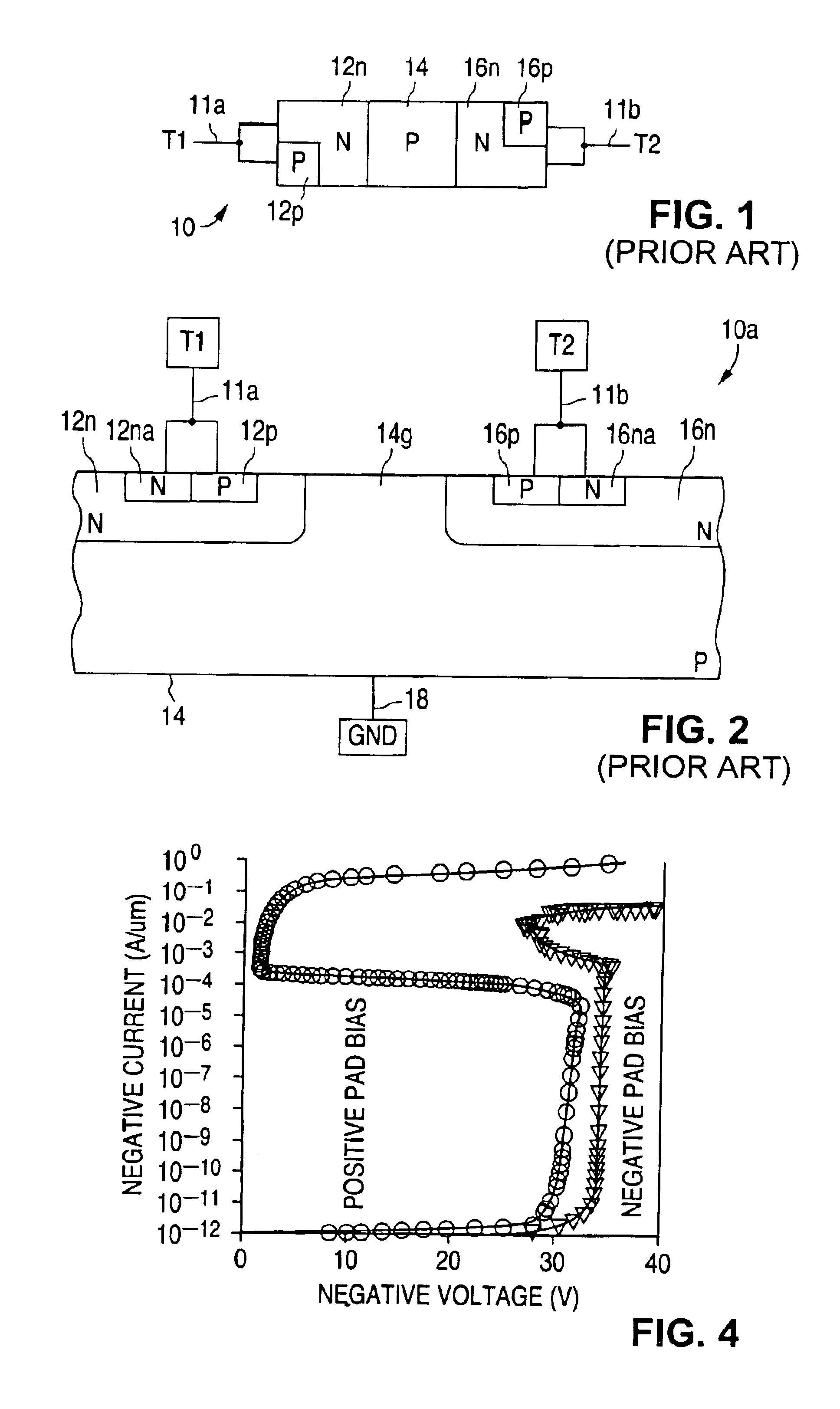
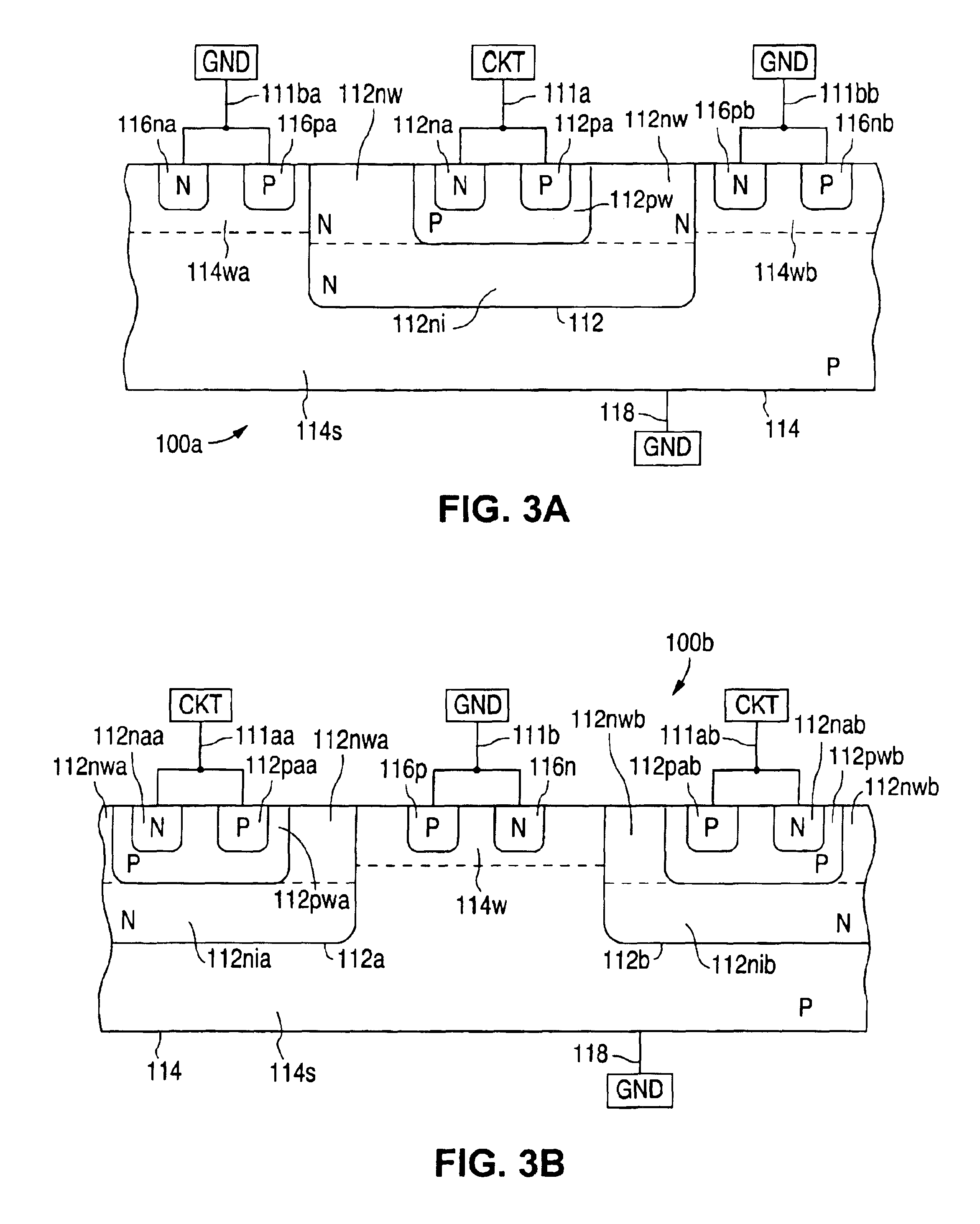
[0019]The following detailed description is of example embodiments of the presently claimed invention with references to the accompanying drawings. Such description is intended to be illustrative and not limiting with respect to the scope of the present invention. Such embodiments are described in sufficient detail to enable one of ordinary skill in the art to practice the subject invention, and it will be understood that other embodiments may be practiced with some variations without departing from the spirit or scope of the subject invention.

[0020]Throughout the present disclosure, absent a clear indication to the contrary from the context, it will be understood that individual circuit elements as described may be singular or plural in number. For example, the terms “circuit” and “circuitry” may include either a single component or a plurality of components, which are either active and / or passive and are connected or otherwise coupled together (e.g., as one or more integrated circ...


PUM


Abstract

An apparatus including an electrostatic discharge (ESD) protection structure with a diac in which substancially similar ESD protection is provided for both positive and negative ESD voltages appearing at the circuit electrode sought to be protected.

Description

BACKGROUND OF THE INVENTION[0001]1. Field of the Invention[0002]The present invention relates to semiconductor circuit structures, and in particular, to semiconductor circuit structures providing electrostatic discharge (ESD) protection for integrated circuits.[0003]2. Description of the Related Art[0004]Electrostatic discharge (ESD) protection devices are widely used in an integrated circuit (IC) to protect the electronic devices within the IC, e.g., bipolar junction transistors (BJTs) and metal oxide semiconductor field effect transistors (MOSFETs), from spurious voltage pulses caused by various sources of electrostatic energy. Numerous conventional ESD protection structures and devices are well known in the art, and include the use of BJTs, MOSFETs, grounded gate metal oxide semiconductor (GGMOS) structures, low voltage triggered silicon controlled rectifiers (LVTSCRs), triacs and diacs.[0005]Electrostatic discharge events produce voltages that typically have large magnitudes and...

Claims


Application Information

Patent Timeline
IPC IPC(8): H01L29/72H01L29/66H01L27/02
CPCH01L27/0259
Inventor VASHCHENKO, VLADISLAVTER BEEK, MARCELHOPPER, PETER J.CONCANNON, ANN
Owner NAT SEMICON CORP
Why Eureka
Try Eureka