Dual-phase delay-locked loop circuit and method

a delay-locked loop and loop circuit technology, applied in the field of integrated circuits, can solve the problems of increasing the time delay introduced by the internal circuitry, the internal clock signal to be phase shifted relative to the external clock signal, and the command applied to the memory device may no longer be valid

Inactive Publication Date: 2005-06-14
MICRON TECH INC
View PDF51 Cites 28 Cited by
  • Summary
  • Abstract
  • Description
  • Claims
  • Application Information

AI Technical Summary

Benefits of technology

[0013]According to one aspect of the present invention, a delay-locked loop, includes a clock multiplier that generates a multiplied clock signal responsive to an input clock signal. The multiplied clock signal has a frequency that is a multiple of a frequency of the input clock signal. A variable delay circuit is coupled to the clock multiplier and generates a delayed clock signal responsive to the multiplied clock signal. The delayed clock signal has a delay relative to the multiplied clock signal and the variable delay circuit controls the value of the delay responsive to a delay control signal. A comparison circuit is coupled to the clock multiplier and to the variable delay circuit to generate the delay control signal in response to the relative phases of the delayed clock signal and the multiplied clock signal.
[0014]According to another aspect of the present invention, a delay-locked loop includes a variable delay circuit that receives an input clock signal and generates a delayed clock signal responsive to the input clock signal. The delayed clock signal has a delay relative to the input clock signal and the variable delay circuit controls the value of the delay responsive to a delay control signal. A comparison circuit is coupled to the variable delay circuit and generates the delay control signal in response to the relative phases of the rising-edge transitions of the delayed and input clock signals and in response to the relative phases of the falling-edge transitions of the delayed and input clock signals.

Problems solved by technology

Internal circuitry in the memory device that generates the internal clock signal necessarily introduces some time delay, causing the internal clock signal to be phase shifted relative to the external clock signal.
As the frequency of the external clock signal increases, however, the time delay introduced by the internal circuitry becomes more significant.
This is true because as the frequency of the external clock signal increases, the period of the signal decreases and thus even small delays introduced by the internal circuitry correspond to significant phase shifts between the internal and external clock signals.
As a result, the commands applied to the memory device may no longer be valid by the time the internal clock signal clocks the latches.
Moreover, although the relative phases of the CLKBUF and CLKFB signals is detected in response to each rising-edge of these signals, the variable delay VD may not be adjusted immediately even where such a phase difference is detected.
As a result, the time it takes to lock the delay-locked loop 100 may slow the operation of the associated synchronous memory device.
Moreover, such a large number of individual delay stages can result in significant power consumption by the delay-locked loop 100, which may be undesirable particularly in applications where synchronous memory device is contained in a portable battery-powered device.

Method used


Image

  • Dual-phase delay-locked loop circuit and method
  • Dual-phase delay-locked loop circuit and method
  • Dual-phase delay-locked loop circuit and method

Examples


Embodiment Construction

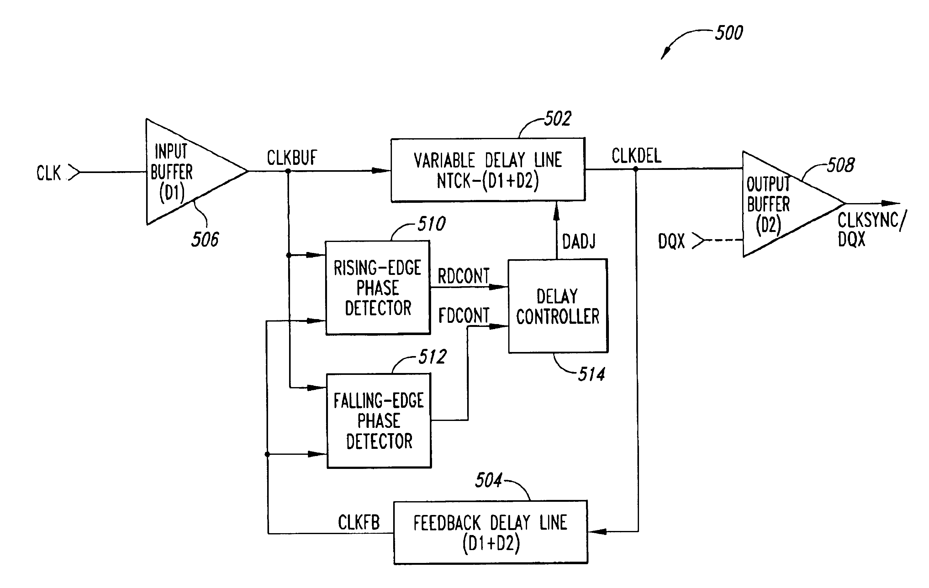
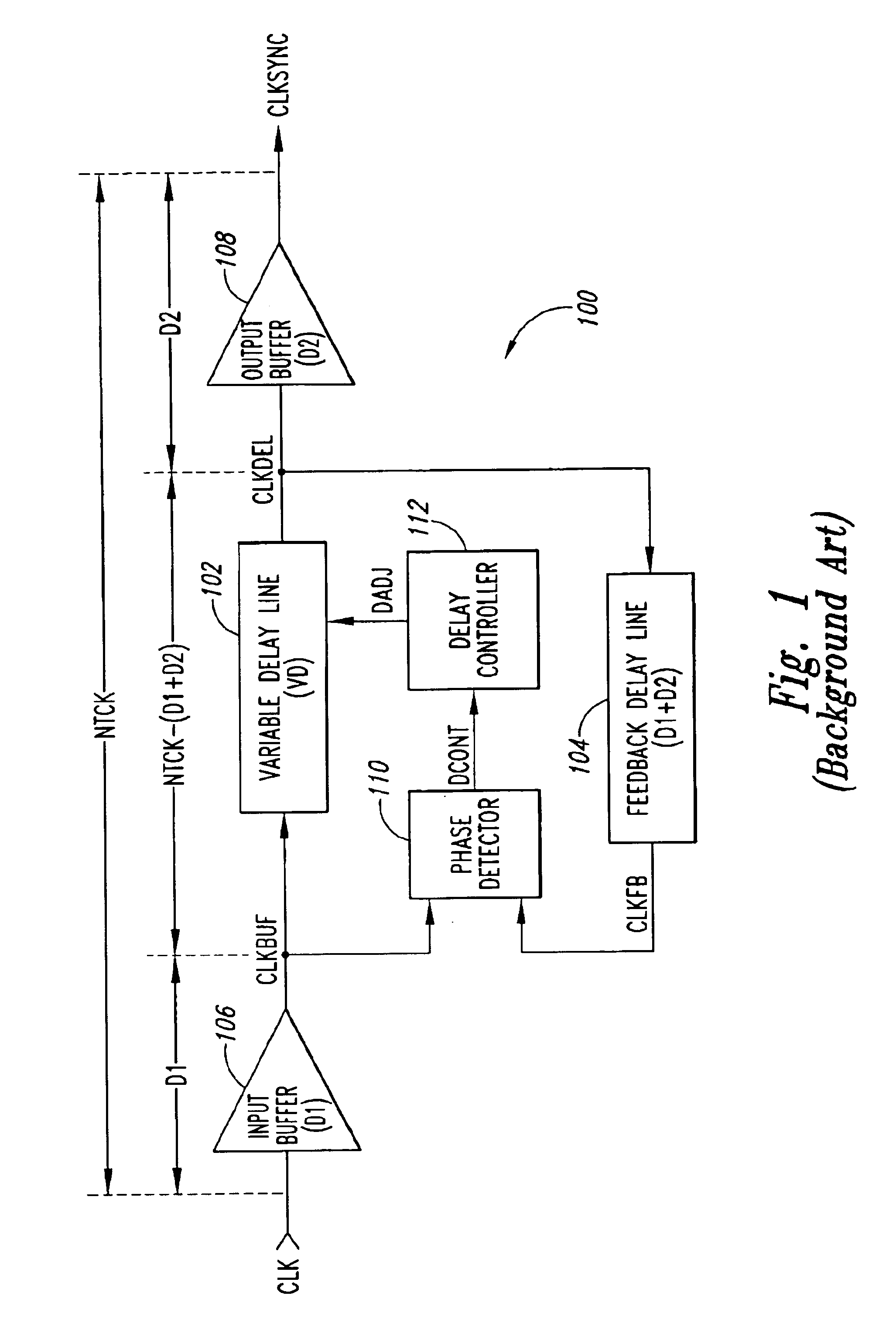
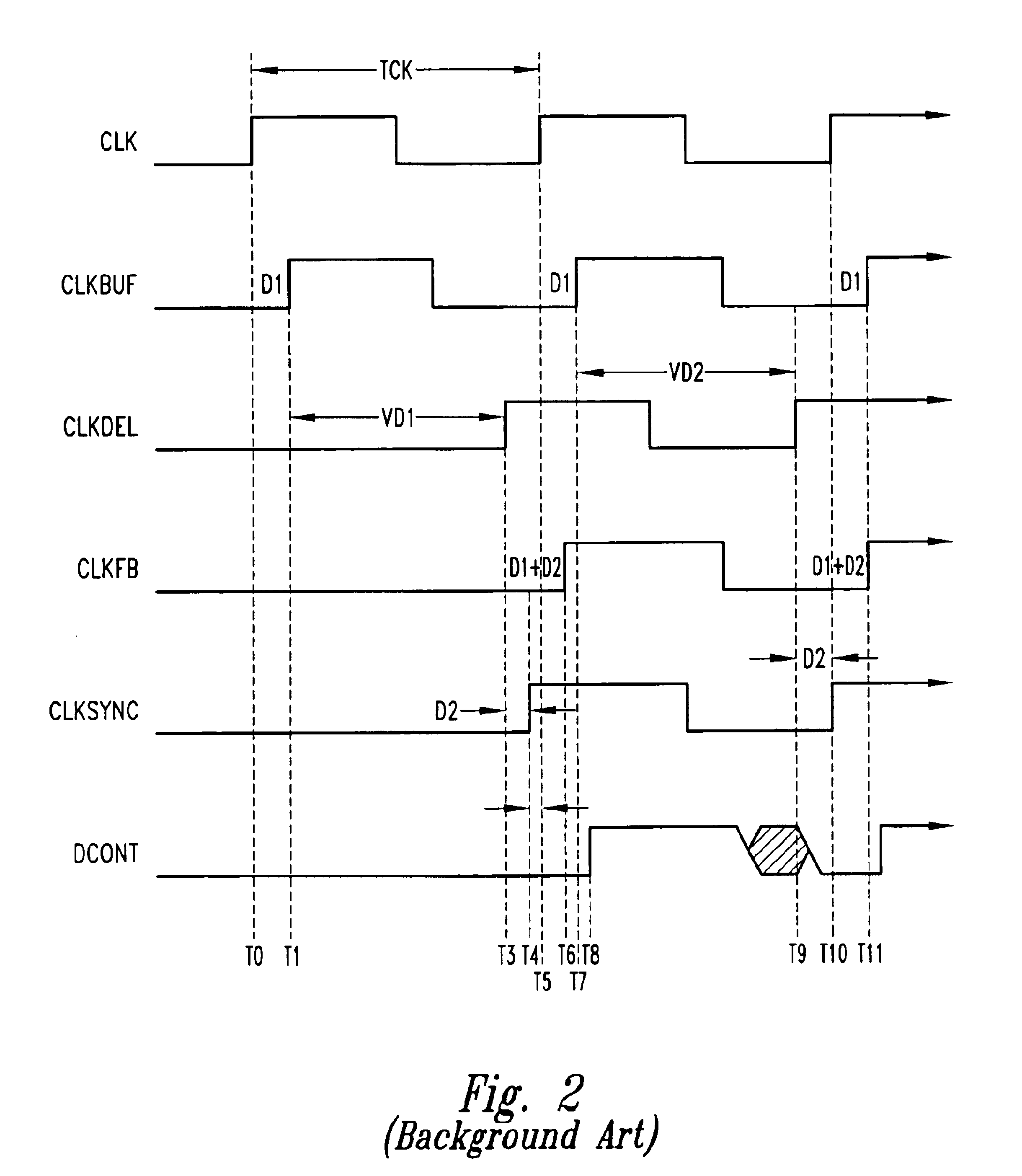
[0024]FIG. 3 is a functional block diagram of a delay-locked loop 300 including a clock multiplier 302 that multiplies a frequency of an applied external clock signal CLK, allowing a variable delay VD of a delayed clock signal CLKDEL to be adjusted multiple times during each cycle of the applied clock signal and thereby enabling the applied clock signal to be more quickly locked, as will be explained in more detail below. In addition to locking more quickly on the CLK signal, the delay-locked loop 300 also enables a smaller variable delay line 304 to be utilized over a given operating frequency range due to the increased frequency of the signal being locked, as will also be explained below in more detail. In the following description, certain details are set forth to provide a sufficient understanding of the invention. It will be clear to one skilled in the art, however, that the invention may be practiced without these particular details. In other instances, well-known circuits, co...


PUM


Abstract

A delay-locked loop includes a clock multiplier that generates a multiplied clock signal responsive to an input clock signal. The multiplied clock signal has a frequency that is a multiple of a frequency of the input clock signal. A variable delay circuit generates a delayed clock signal responsive to the multiplied clock signal, the delayed clock signal having a delay relative to the multiplied clock signal. The variable delay circuit controls the value of the delay responsive to a delay control signal. A comparison circuit generates the delay control signal in response to the relative phases of the delayed clock signal and the multiplied clock signal. In another embodiment, the delay-locked loop omits the clock multiplier and instead includes a comparison circuit that generates the delay control signal in response to the relative phases of both the rising- and falling-edge transitions of the delayed and input clock signals.

Description

CROSS-REFERENCE TO RELATED APPLICATION[0001]This application is a divisional of pending U.S. patent application Ser. No. 09 / 974,386, filed Oct. 9, 2001.TECHNICAL FIELD[0002]The present invention relates generally to integrated circuits, and more specifically to synchronizing an external clock signal applied to an integrated circuit with internal clock signals generated in the integrated circuit in response to the external clock signal.BACKGROUND OF THE INVENTION[0003]In synchronous integrated circuits, the integrated circuit is clocked by an external clock signal and performs operations at predetermined times relative the rising and falling edges of the applied clock signal. Examples of synchronous integrated circuits include synchronous memory devices such as synchronous dynamic random access memories (SDRAMs), synchronous static random access memories (SSRAMs), and packetized memories like SLDRAMs and RDRAMs, and include other types of integrated circuits as well, such as micropro...

Claims


Application Information

Patent Timeline
Patent Type & Authority Patents(United States)
IPC IPC(8): H01L31/0264H01L31/0328H03L7/06H03L7/081H03L7/087
CPCH03L7/087H03L7/0812H03L7/0816
Inventor DREXLER, ADRIAN J.
Owner MICRON TECH INC
Why Eureka
Try Eureka