

Method for manufacturing and packaging integrated circuit
- Summary
- Abstract
- Description
- Claims
- Application Information
AI Technical Summary
Benefits of technology
Problems solved by technology
Method used
Image

Examples
Embodiment Construction
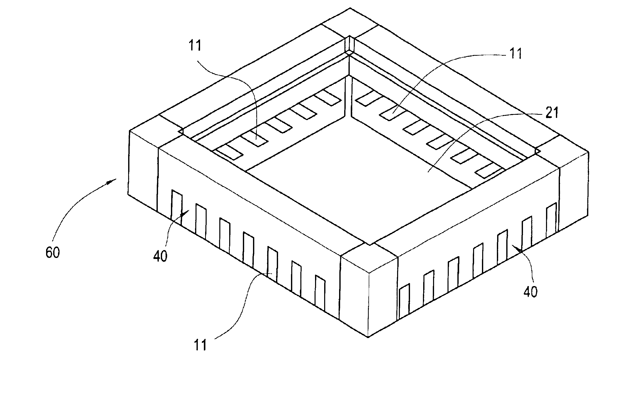
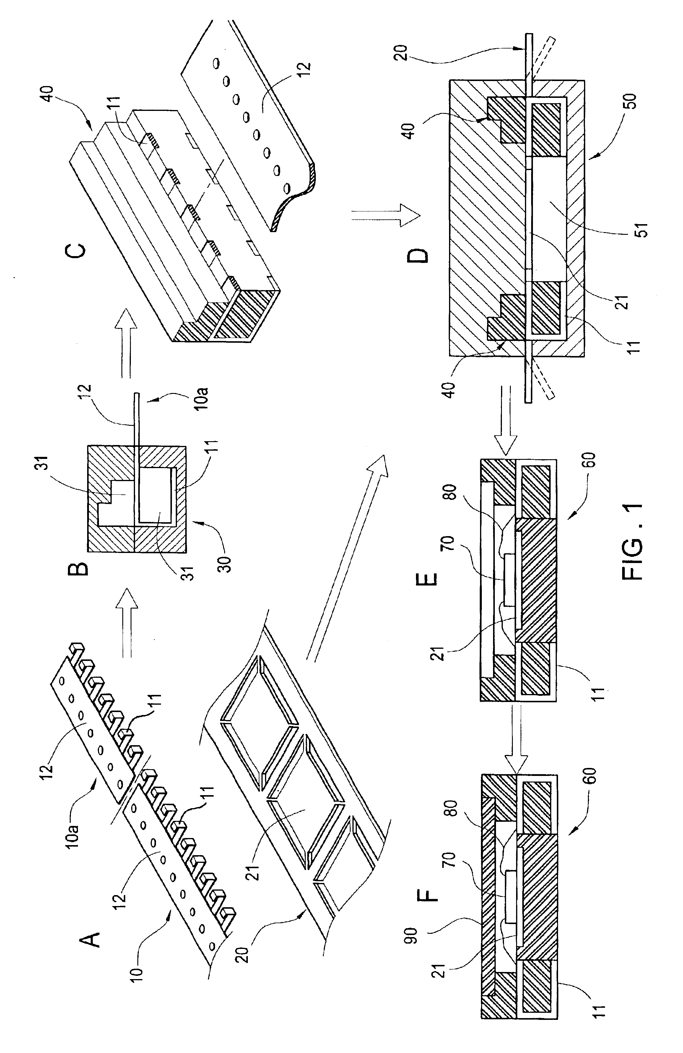
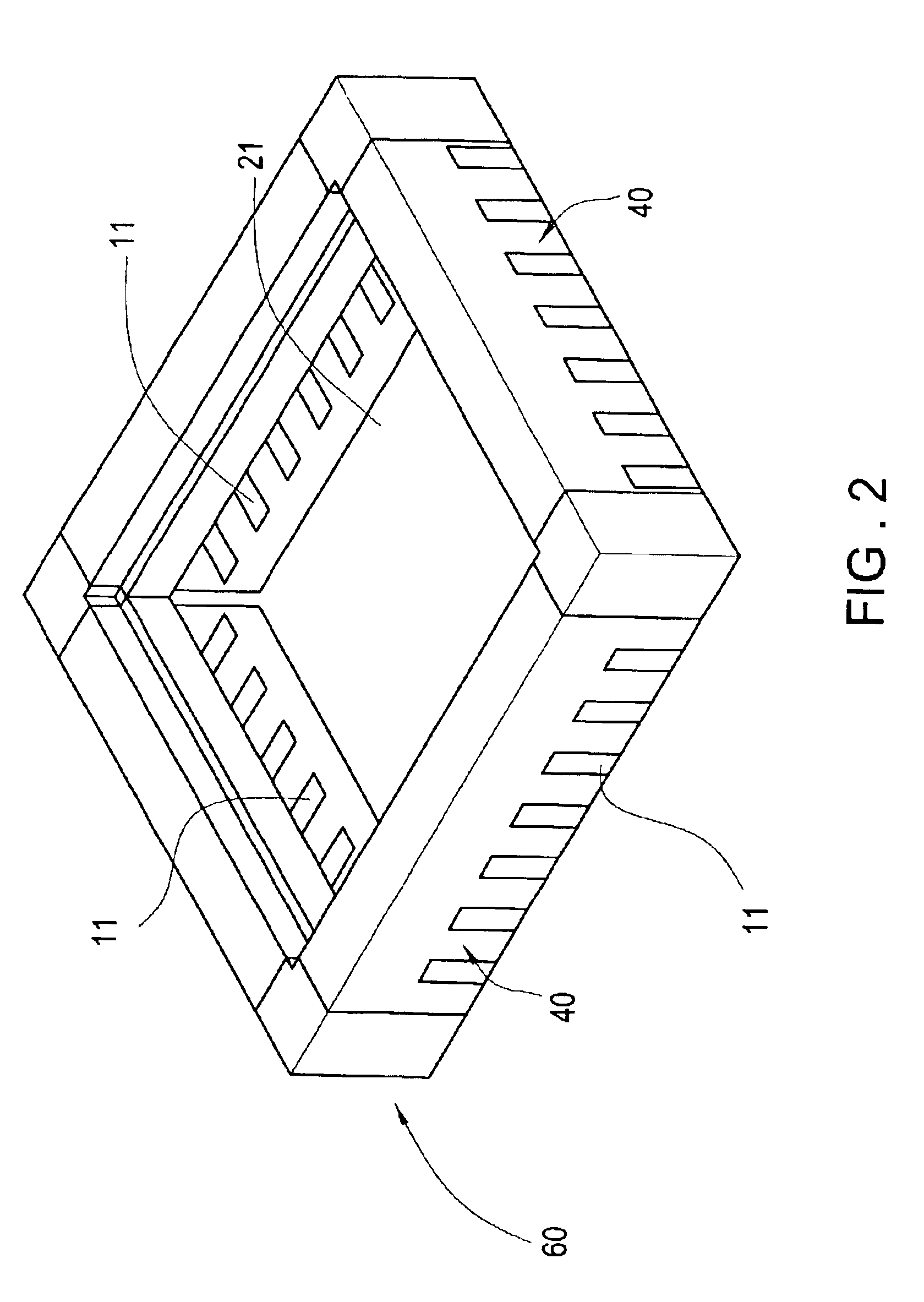
[0017]At first, please refer to FIG. 1 and FIG. 2, a method for manufacturing and packaging an integrated circuit includes following procedures:[0018](a) Pressure a continuous pin material area 10 and a base board area 20, on the pin material area 10 lined up several pins 11 (as for this example, the pins look like “L” type perpendicular to pin material area); whereas at the center of the base board area 20 possesses a plurality of base board 21;[0019](b) Cut off pin material area 10 into a plurality of pin units 10a (each IC is composed of four pin units) with pin 11 number (length) required, then accommodate each pin units into respective position in the mould 30;[0020](c) then eject plastic to fill mould gap 31 of the mould 30 into one pin unit 40, and then cut off waste part 12 of pin material area 10 after tearing down the mould parts;[0021](d) Put four pin units 40 and one base board area 20 mentioned above into the four edge and center of a rectangle mould 50 respectively, th...
PUM
| Property | Measurement | Unit |
|---|---|---|
| Time | aaaaa | aaaaa |
Abstract
Description
Claims
Application Information