Wafer bevel edge cleaning system and apparatus
- Summary
- Abstract
- Description
- Claims
- Application Information
AI Technical Summary
Benefits of technology
Problems solved by technology
Method used
Image

Examples
Embodiment Construction
[0050]Several exemplary embodiments for an improved and more effective and more flexible wafer edge cleaning system, method and apparatus will now be described. It will be apparent to those skilled in the art that the present invention may be practiced without some or all of the specific details set forth herein.
[0051]Wafer edge cleaning systems and methods are very important to the ultimate quality of the resulting semiconductor. One embodiment includes an edge cleaning system, method and apparatus that have separate cleaning of the front side edge zone and the back side edge zone. Separating and decoupling the front side edge zone cleaning from the back side edge zone cleaning allows for a more flexible and effective bevel edge and edge zone cleaning process and also allows more effective control of the bevel edge and edge zone cleaning process.
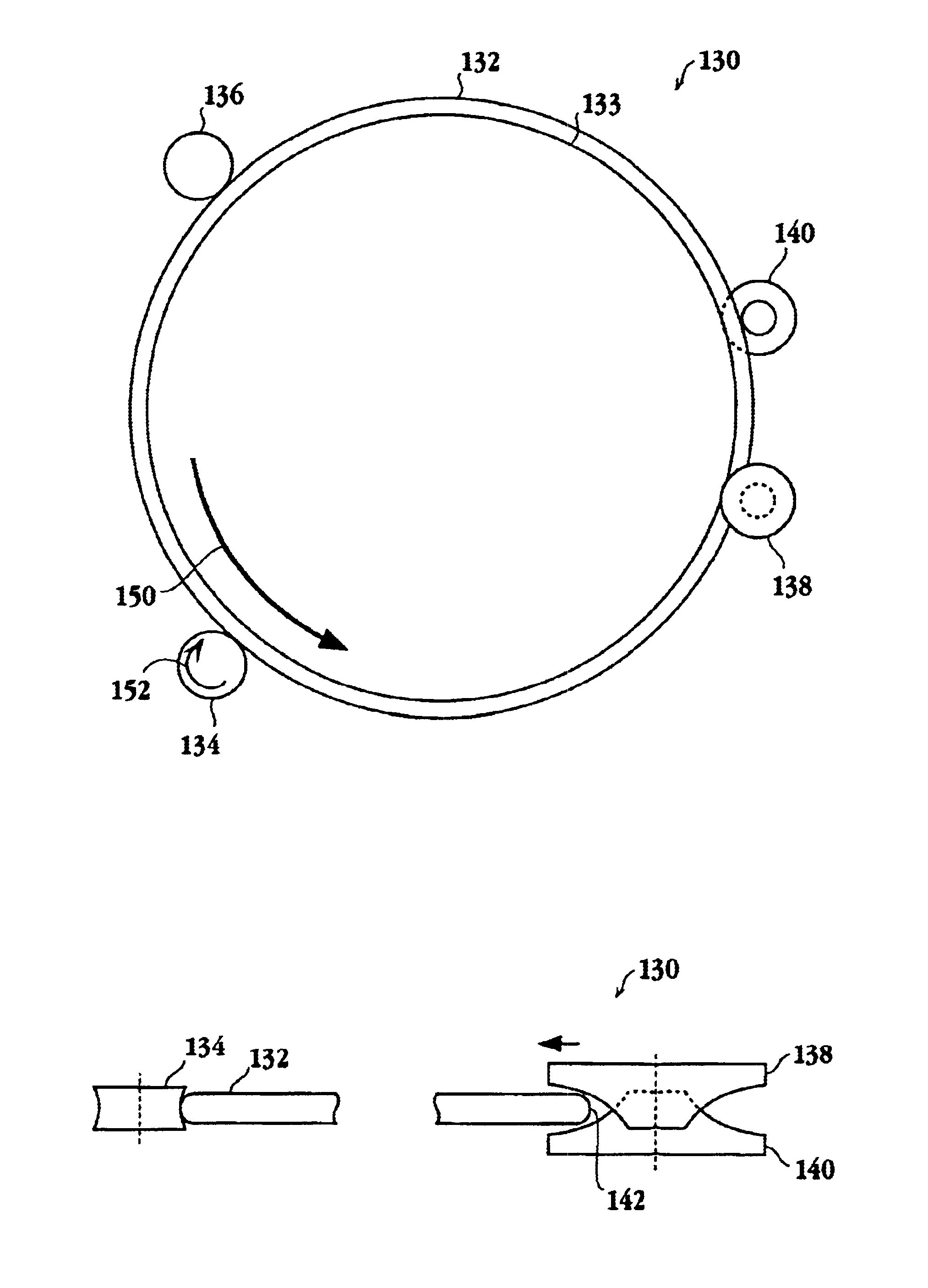
[0052]FIGS. 2A and 2B show a side view and a top view, respectively, of a cleaning system 120 in accordance with one embodiment of the pre...
PUM
 Abstract
Description
Claims
Application Information
 - R&D
- Intellectual Property
- Life Sciences
- Materials
- Tech Scout
- Unparalleled Data Quality
- Higher Quality Content
- 60% Fewer Hallucinations
Browse by: Latest US Patents, China's latest patents, Technical Efficacy Thesaurus, Application Domain, Technology Topic, Popular Technical Reports.
© 2025 PatSnap. All rights reserved.Legal|Privacy policy|Modern Slavery Act Transparency Statement|Sitemap|About US| Contact US: help@patsnap.com