Two-dimensional scatter plot technique for defect inspection

a defect inspection and two-dimensional scattering technology, applied in the field of digital image processing, can solve problems such as nuisance defects adversely affecting production throughput, important but imprecise tasks,

Inactive Publication Date: 2005-06-28
APPLIED MATERIALS INC
View PDF22 Cites 12 Cited by
  • Summary
  • Abstract
  • Description
  • Claims
  • Application Information

AI Technical Summary

Problems solved by technology

Finding the optimum threshold value for a given test image is an important but imprecise task.
Nuisance

Method used


Image

  • Two-dimensional scatter plot technique for defect inspection
  • Two-dimensional scatter plot technique for defect inspection
  • Two-dimensional scatter plot technique for defect inspection

Examples


Embodiment Construction

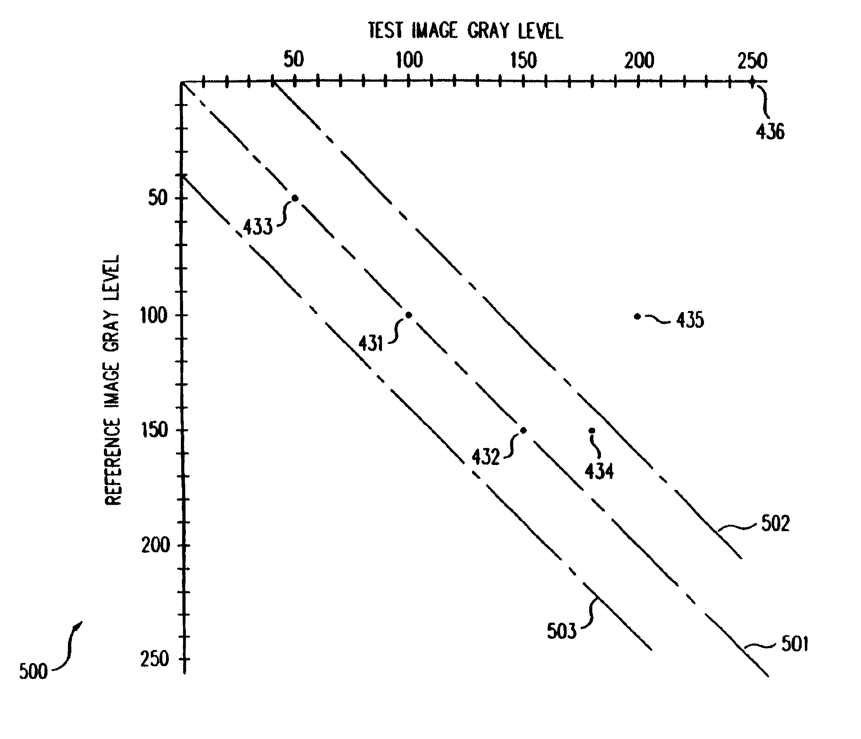
[0017]The present invention provides for a method and associated apparatus for relating the pixel of a test image with the corresponding pixel on a reference image. The invention can be used in determining the effectiveness of a threshold or thresholding scheme. The invention is also useful in other image processing applications such as those disclosed by the same inventor in the related co-pending U.S. patent application Ser. No. 09 / 365,503 filed Aug. 2, 1999, “Adaptive Mask Technique For Defect Inspection,” which is incorporated herein by reference in its entirety. Other uses for the invention are in electron-beam, bright-field, dark-field, laser, and atomic-force microscopy (“AFM”) inspection systems.

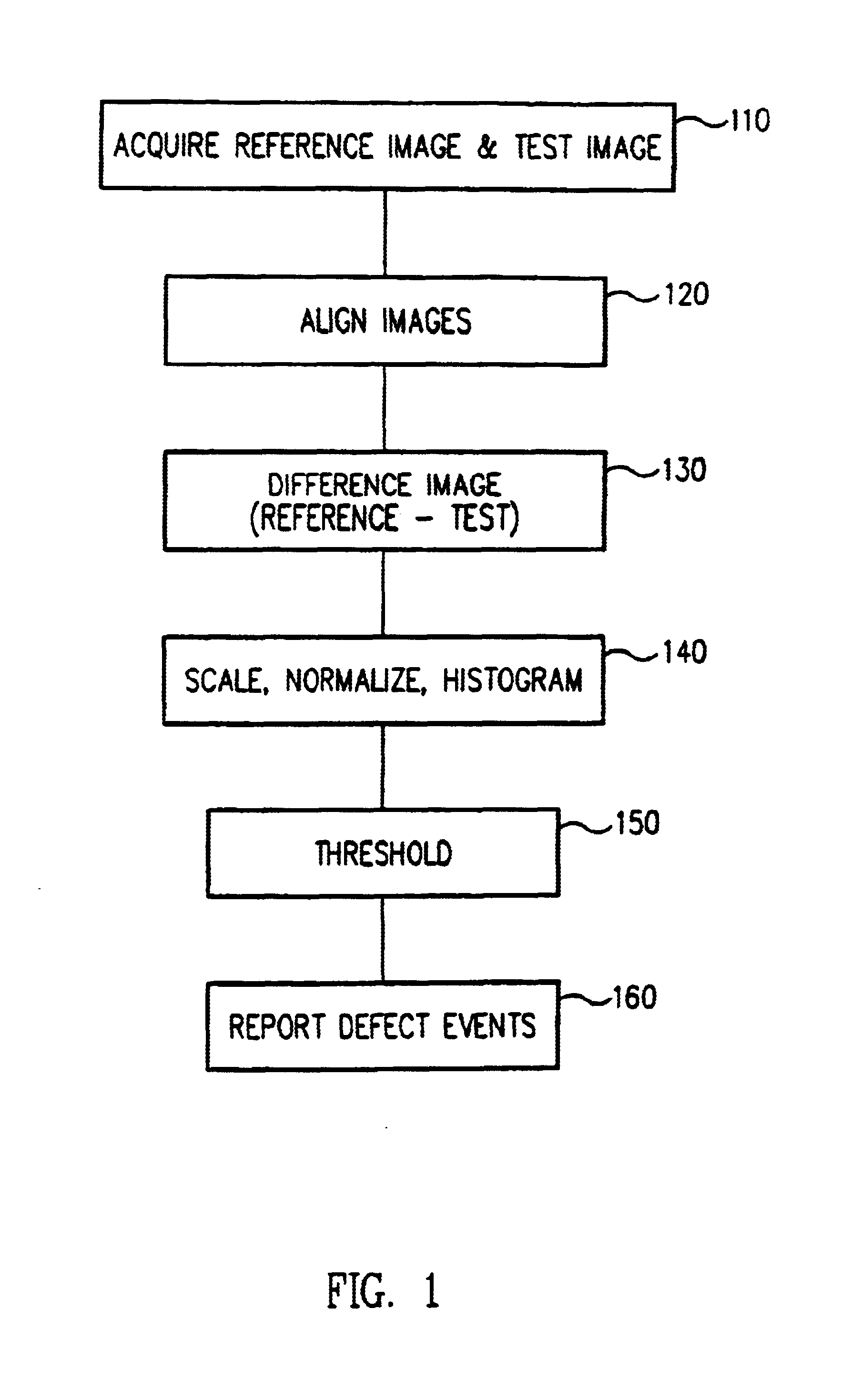
[0018]FIG. 3. illustrates the steps of an embodiment of the present invention. In step 310, a test image and a reference image of, for example, semiconductor structures are acquired using conventional image acquisition techniques. The images can also be acquired using the step-and-im...


PUM


Abstract

A method and associated apparatus for relating a test image with a reference image in an automated image processing system is disclosed. The test and reference images are aligned. A two-dimensional scatter plot is then created by plotting the gray level of a test image pixel against the gray level of a corresponding reference image pixel for each aligned pixel location.

Description

COPYRIGHT NOTICE[0001]A portion of the disclosure of this patent document contains material which is subject to copyright protection. The copyright owner has no objection to the facsimile reproduction by anyone of the patent document or the patent disclosure, as it appears in the Patent and Trademark Office patent file or records, but otherwise reserves all copyright rights whatsoever. 37 CFR 1.71(e).BACKGROUND OF THE INVENTION[0002]1. Field of the Invention[0003]This invention generally relates to digital image processing and, more particularly, to systems and methods for detecting defects in a semiconductor device using image comparison techniques.[0004]2. Description of the Related Art[0005]Image comparison techniques are used to detect defects in a semiconductor wafer. Typically, a test image is acquired and then compared to a reference image. A defect-detection algorithm is then used to detect variations between the images and to determine whether such variations are real defec...

Claims


Application Information

Patent Timeline
IPC IPC(8): G06T7/00G06T1/00H01L21/66
CPCG06T7/001G06T7/0024G06T2207/30148G06T7/30G06T7/00
Inventor AGHAJAN, HAMID K.
Owner APPLIED MATERIALS INC
Why Eureka
Try Eureka