Electrooptical device substrate, electrooptical device, methods for fabricating electrooptical device substrate and electrooptical device, electronic apparatus, and method for tuning color of color filter

a technology of electrooptical devices and substrates, applied in the direction of optics, optical filters, instruments, etc., can solve the problems of increasing material costs, unable to optimize the colors of transmissive display and reflective display at the same time, and unable to achieve the effect of reducing the differences in the degrees of both chroma and hue between a reflective display and a transmissive display

Inactive Publication Date: 2005-08-09
BOE TECH GRP CO LTD
View PDF8 Cites 19 Cited by
  • Summary
  • Abstract
  • Description
  • Claims
  • Application Information

AI Technical Summary

Benefits of technology

[0013]In order to solve the foregoing problems, in an electrooptical device substrate and an electrooptical device, and by methods for fabricating them according to the present invention, coloring layers, each having a hypochromic portion and a hyperchromic portion having a higher light density than the hypochromic portion, and a reflective layer including apertures are formed, wherein the hypochromic portion is disposed so as to two-dimensionally overlap the reflective layer and the hyperchromic portion is disposed so as to two-dimensionally overlap the corresponding aperture. With this structure, in the coloring layer having the hypochromic portion and the hyperchromic portion, since the hyperchromic portion is disposed at least above the corresponding aperture of the reflective layer, light passing through the corresponding aperture of the reflective layer is transmitted through the hyperchromic portion. Accordingly the chroma of transmitted light can be improved compared to what is possible today, and also the differences in the degrees of both the chroma and the hue between a reflective display and a transmissive display can be reduced.

Problems solved by technology

However, when the color of the liquid crystal display is to be tuned in the foregoing known liquid crystal panel, it is required to prepare photosensitive agents in which the amounts of colorants such as pigments are finely adjusted in order to achieve the desired display color, thereby increasing the material cost and requiring a lot of work for preparing the photosensitive agents.
In particular, in the foregoing transflective liquid crystal display panel, since the colors of the transmissive display and the reflective display are different from each other, optimizing the colors of the transmissive display and the reflective display at the same time is impossible.
Accordingly, the display colors are set in a moderately compromised manner, thereby giving rise to problems in that improving the display quality of the liquid crystal display panel is difficult and that the foregoing tuning work of the color becomes troublesome burden when the liquid crystal display panel is fabricated.
More particularly, since the brightness of the reflective display generally tends to be insufficient, it is necessary to set the color filter 112 so as to have a high light transmission in order to maintain the brightness thereof; however, this arrangement causes the transmissive display to have an insufficient chroma.
Moreover, as described above, the number of times the light passes through the color filter in the reflective display is different from that in the transmissive display, and thus the perceived color of the reflective display is dramatically different from that of transmissive display, thereby detracting from the appearance.

Method used


Image

  • Electrooptical device substrate, electrooptical device, methods for fabricating electrooptical device substrate and electrooptical device, electronic apparatus, and method for tuning color of color filter
  • Electrooptical device substrate, electrooptical device, methods for fabricating electrooptical device substrate and electrooptical device, electronic apparatus, and method for tuning color of color filter
  • Electrooptical device substrate, electrooptical device, methods for fabricating electrooptical device substrate and electrooptical device, electronic apparatus, and method for tuning color of color filter

Examples


first embodiment

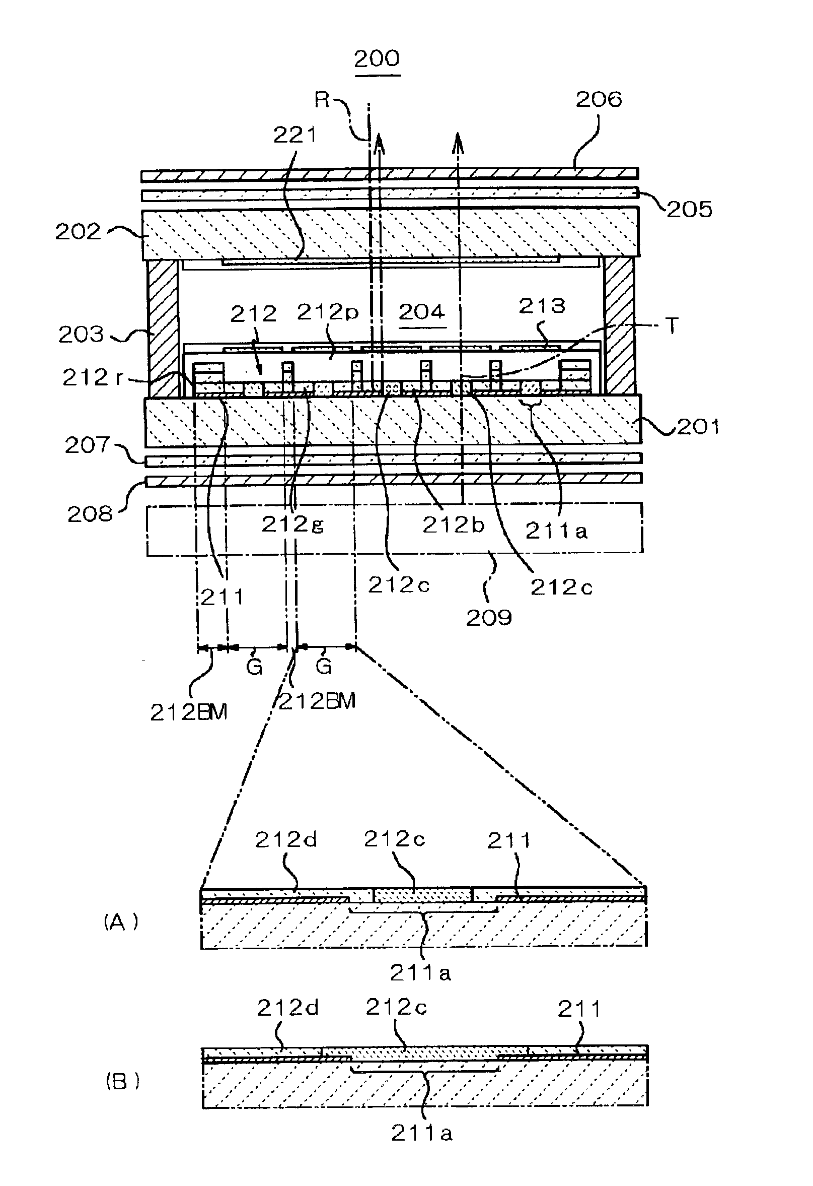
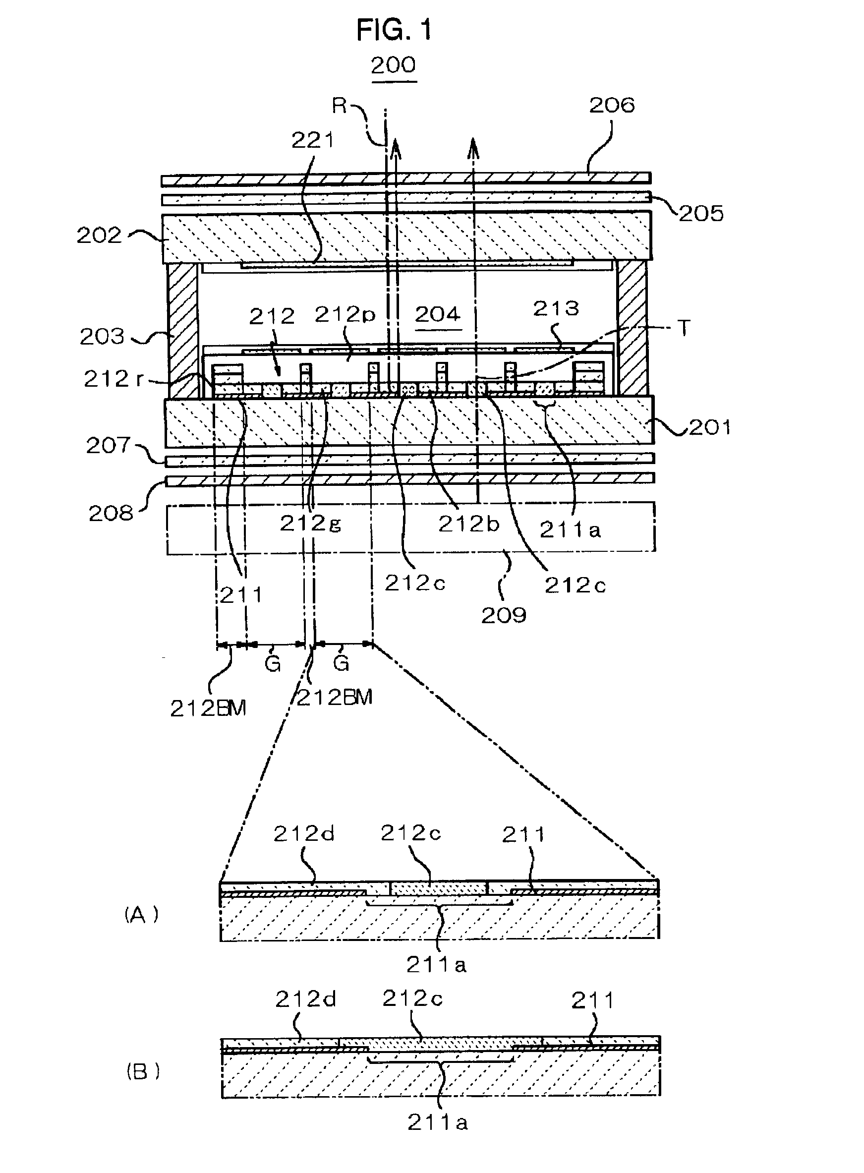
[0087]FIG. 1 is a schematic sectional view illustrating a substrate 210 which is an electrooptical device substrate according to a first embodiment of the present invention and a liquid crystal display panel 200 of an electrooptical device using the electrooptical device substrate according to the first embodiment.

[0088]The liquid crystal display panel 200 is constructed such that the substrate 201 and a substrate 202 composed of glass, plastic, or the like are bonded to each other with sealing adhesive 203, and liquid crystal 204 is injected into the space formed therebetween. Transparent electrodes 221, retardation films 205 and 207, and polarizers 206 and 208 formed on the substrate 202 are completely identical to those of the foregoing known example shown in FIG. 11.

[0089]In this embodiment, the substrate 201 has a reflective layer 211, having apertures 211a, formed on the inner surface thereof in the same fashion as the known example. The reflective layer 211 is formed of a thi...

second embodiment

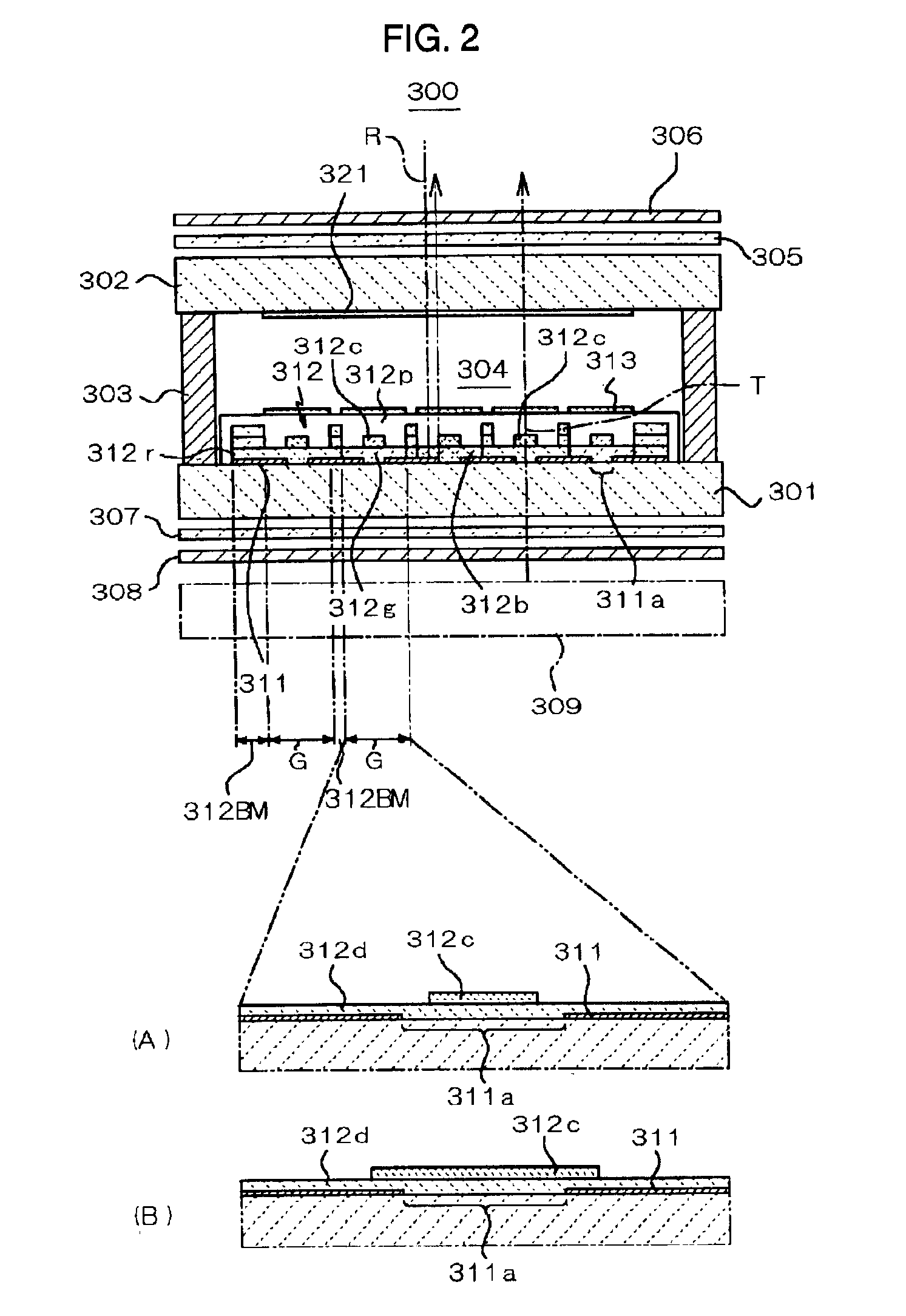
[0106]Referring now to FIG. 2, an electrooptical device substrate 301 and a liquid crystal display panel 300 according to a second embodiment of the present invention will be described. In this embodiment, since the substrate 301, a substrate 302, sealing adhesive 303, liquid crystal 304, transparent electrodes 313 and 321, retardation films 305 and 307, and polarizers 306 and 308 are provided in a similar fashion to the first embodiment, a repeated description thereof will be omitted.

[0107]In this embodiment, the substrate 301 has a reflective layer 311 having apertures 311a on the surface thereof, and the reflective layer 311 has coloring layers 312r, 312g, and 312b formed thereon, one coloring layer disposed at each pixel. Each coloring layer is formed in the overall corresponding pixel so as to cover the corresponding aperture 311a. The coloring layer has a hypochromic portion 312d, formed on the foregoing reflective layer 311 over the whole pixel (refer to FIG. 2(A) or 2(B)), a...

third embodiment

[0112]Referring now to FIG. 3, an electrooptical device substrate 410 and a liquid crystal display panel 400 according to a third embodiment of the present invention will be described. Also, in this embodiment, since the substrate 401, a substrate 402, sealing adhesive 403, liquid crystal 404, transparent electrodes 413 and 421, retardation films 405 and 407, and polarizers 406 and 408 are provided in a similar fashion to the first embodiment, a repeated description thereof will be omitted.

[0113]Also, in this embodiment, the substrate 401 has a reflective layer 411 thereon having apertures 411a, and the reflective layer 411 has a color filter 412, directly formed thereon, having coloring layers 412r, 412g, and 412b, a stacked black matrix 412BM, and an overcoat film 412p, in a similar fashion to the foregoing embodiments.

[0114]In this embodiment, the substrate 401 has hyperchromic portions 412c formed thereon, one disposed at each pixel and serving as a part of each of the foregoing...


PUM

PropertyMeasurementUnit
hypochromicaaaaaaaaaa
colorsaaaaaaaaaa
structureaaaaaaaaaa

Abstract

A substrate 201 has a reflective layer 211 thereon having apertures 211a, and the reflective layer has a color filter 212 thereon having coloring layers 212r, 212g, 212b. One coloring layer at each pixel has a hyperchromic portion 212c above the corresponding aperture 211a of the reflective layer 211, and a hypochromic portion 212d on the reflective layer 211. There is a region in which no hyperchromic portion 212c is disposed above the corresponding aperture 211a (FIG. 1(A)) or another region in which no hypochromic portion 212d is disposed on the reflective layer 211 (FIG. 1(B)).

Description

BACKGROUND OF THE INVENTION[0001]1. Technical Field of the Invention[0002]The present invention relates to electrooptical device substrates, electrooptical devices, methods for fabricating the electrooptical device substrates and the electrooptical devices, and methods for tuning the colors of color filters, and more particularly, the present invention relates to a structure of a color filter suitable for a transflective electrooptical device.[0003]2. Description of the Related Art[0004]Hitherto, in known transflective liquid crystal display panels, both a reflective display using external light and a transmissive display using illuminating light such as backlight are made visible. All transflective liquid crystal display panels have a reflective layer therein for reflecting external light and have a structure in which illuminating light such as light from a backlight passes through the reflective layer. Some reflective layers of this type have a pattern in which one aperture (one s...

Claims


Application Information

Patent Timeline
Patent Type & Authority Patents(United States)
IPC IPC(8): G02B5/20G02F1/1335
CPCG02F1/133514G02F1/133555G02F1/1335
Inventor TAKIZAWA, KEIJI
Owner BOE TECH GRP CO LTD
Why Eureka
Try Eureka