End point detection with imaging matching in semiconductor processing

a technology of end point detection and semiconductor processing, applied in the field of semiconductor processing, can solve the problems of inability to achieve repeatable endpoint detection granularity, inability to achieve repeatable endpoint detection, and significant amount of processing required to translate spectral data to a single valu

Inactive Publication Date: 2005-08-16
LAM RES CORP
View PDF58 Cites 47 Cited by
  • Summary
  • Abstract
  • Description
  • Claims
  • Application Information

AI Technical Summary

Benefits of technology

[0008]The present invention includes a system for endpoint detection. The endpoint detection system detects one or more desired states of processing of prod

Problems solved by technology

One drawback to this form of endpoint detection is the significant amount of processing required to translate spectral data to a single value that is an endpoint signal.
In addition, due to averaging, ratios and/or other processing of the spectral data to obtain the endpoint sign

Method used


Image

  • End point detection with imaging matching in semiconductor processing
  • End point detection with imaging matching in semiconductor processing
  • End point detection with imaging matching in semiconductor processing

Examples


Embodiment Construction

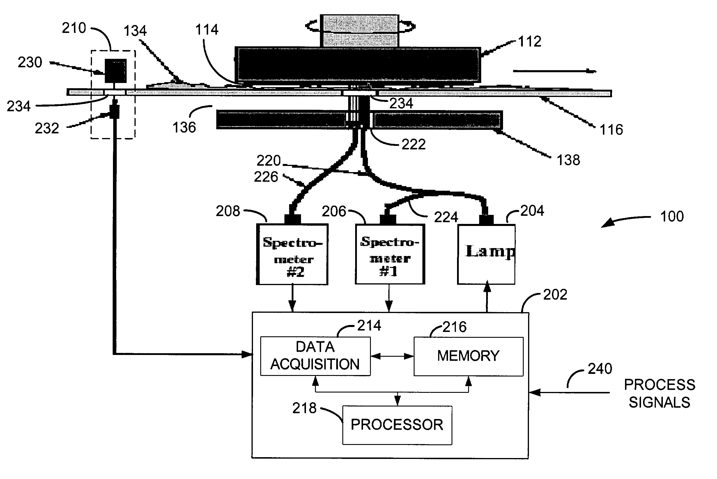
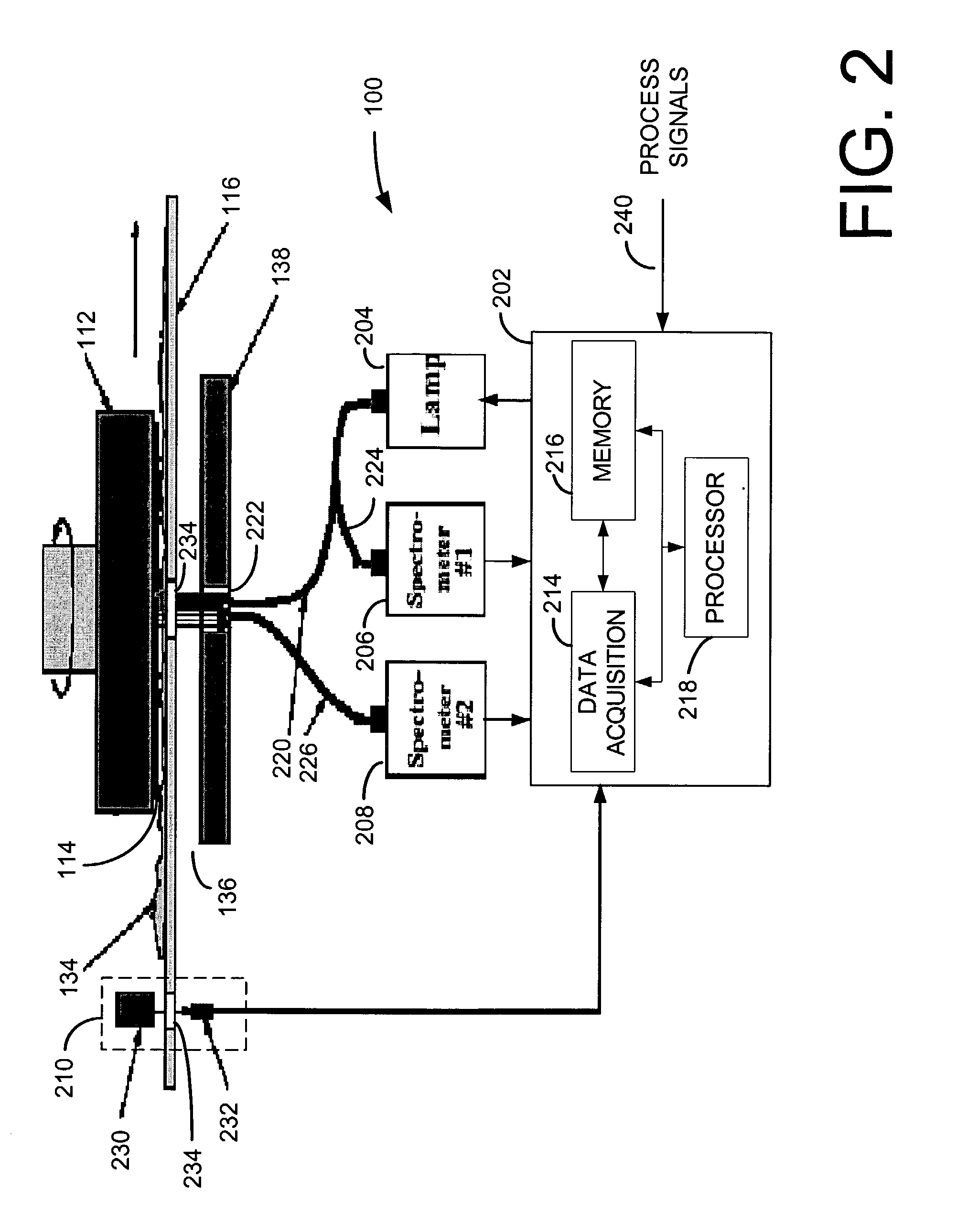
[0026]The present invention includes an endpoint detection system. The endpoint detection system may provide accurate endpoint determination / thickness determination for semiconductor wafer processing. Endpoint determination may be performed with the endpoint detection system by dynamic in-situ capture of process related data. The process related data may be indicative of the current state of processing of a semiconductor wafer. The endpoint detection system may utilize captured and / or generated process related data to develop a production image. During processing the production image may be compared with a reference image to determine a desired state of processing of the production semiconductor wafer, such as endpoint and / or wafer thickness. The endpoint detection system may provide indications and / or control signals when the production image and the reference image are substantially similar.

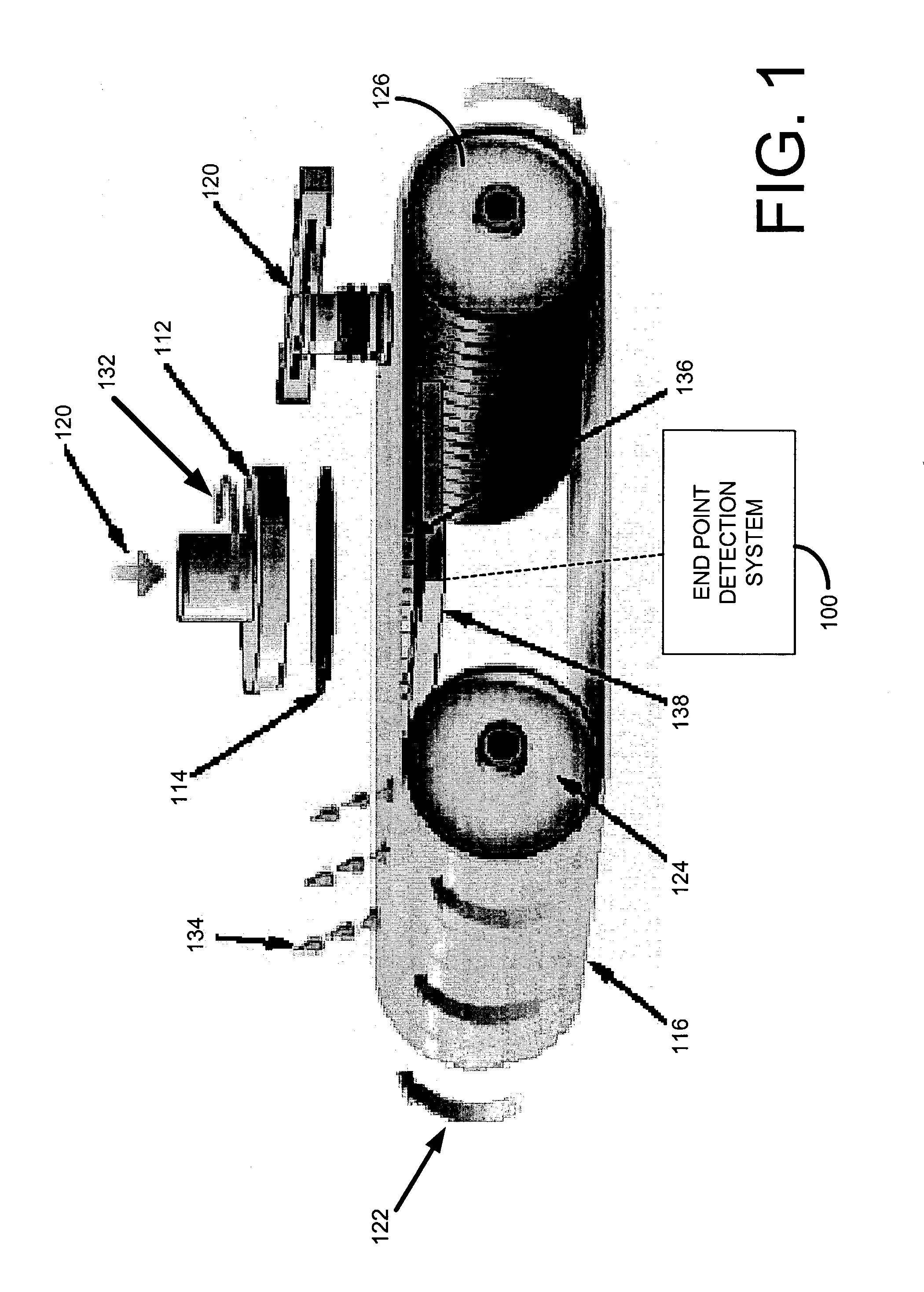
[0027]FIG. 1 is a perspective view of an example semiconductor processing machine that incl...


PUM


Abstract

An end point detection system may compare a production image developed during processing of production semiconductor wafer with a reference image. The reference image is representative of a desired state of processing of the production semiconductor wafer. The reference image is determined by processing a reference semiconductor wafer. The reference semiconductor wafer may be part of a wafer group of similar wafers that includes the production semiconductor wafer. The end point detection system may dynamically develop the production image during processing of the production semiconductor wafer. Indication may be provided by the end point detection system when the reference image and the production image are substantially similar.

Description

BACKGROUND OF THE INVENTION[0001]1. Technical Field[0002]The present invention relates generally to semiconductor processing, and more particularly, to end point detection in semiconductor processing using image matching.[0003]2. Related Art[0004]Chemical Mechanical Polishing (CMP) is a well known process for polishing semiconductor wafers. In general, a semiconductor wafer is placed in frictional contact with a moving polishing pad to remove material from the surface of the wafer. The material is typically removed until a desired thickness of the semiconductor wafer is achieved and the polishing process is then terminated. The determination of when to terminate the polishing process is referred to as endpoint detection (EPD).[0005]EPD may take a variety of forms all with the ultimate goal of achieving uniformity among different semiconductor wafers even though process and material variations continuously occur during the polishing process. One category of EPD techniques are known a...

Claims


Application Information

Patent Timeline
IPC IPC(8): G01B9/02B24B21/04B24B37/04B24B49/12G01N21/956G06T7/00
CPCB24B21/04B24B37/013B24B37/04B24B49/12G06T7/001G06T7/004G01N21/95607G06T2207/30148G06T7/70
Inventor YI, JINGANGXU, CANGSHAN
Owner LAM RES CORP
Why Eureka
Try Eureka