Output driving circuit for maintaining I/O signal duty ratios

Inactive Publication Date: 2005-08-23
LG ELECTRONICS INC
View PDF1 Cites 19 Cited by
  • Summary
  • Abstract
  • Description
  • Claims
  • Application Information

AI Technical Summary

Benefits of technology

[0026]An object of the present invention is to provide an output driving circuit which can maintain duty ratios of input/output signals constant.
[0027]Another object

Problems solved by technology

There has been a problem in that the level shifter can not be used for an integrated circuit operative at a fast speed.
Therefore, when a voltage level of a signal is shifted and provided to the outside of the inte

Method used


Image

  • Output driving circuit for maintaining I/O signal duty ratios
  • Output driving circuit for maintaining I/O signal duty ratios
  • Output driving circuit for maintaining I/O signal duty ratios

Examples


first embodiment

1) First Embodiment

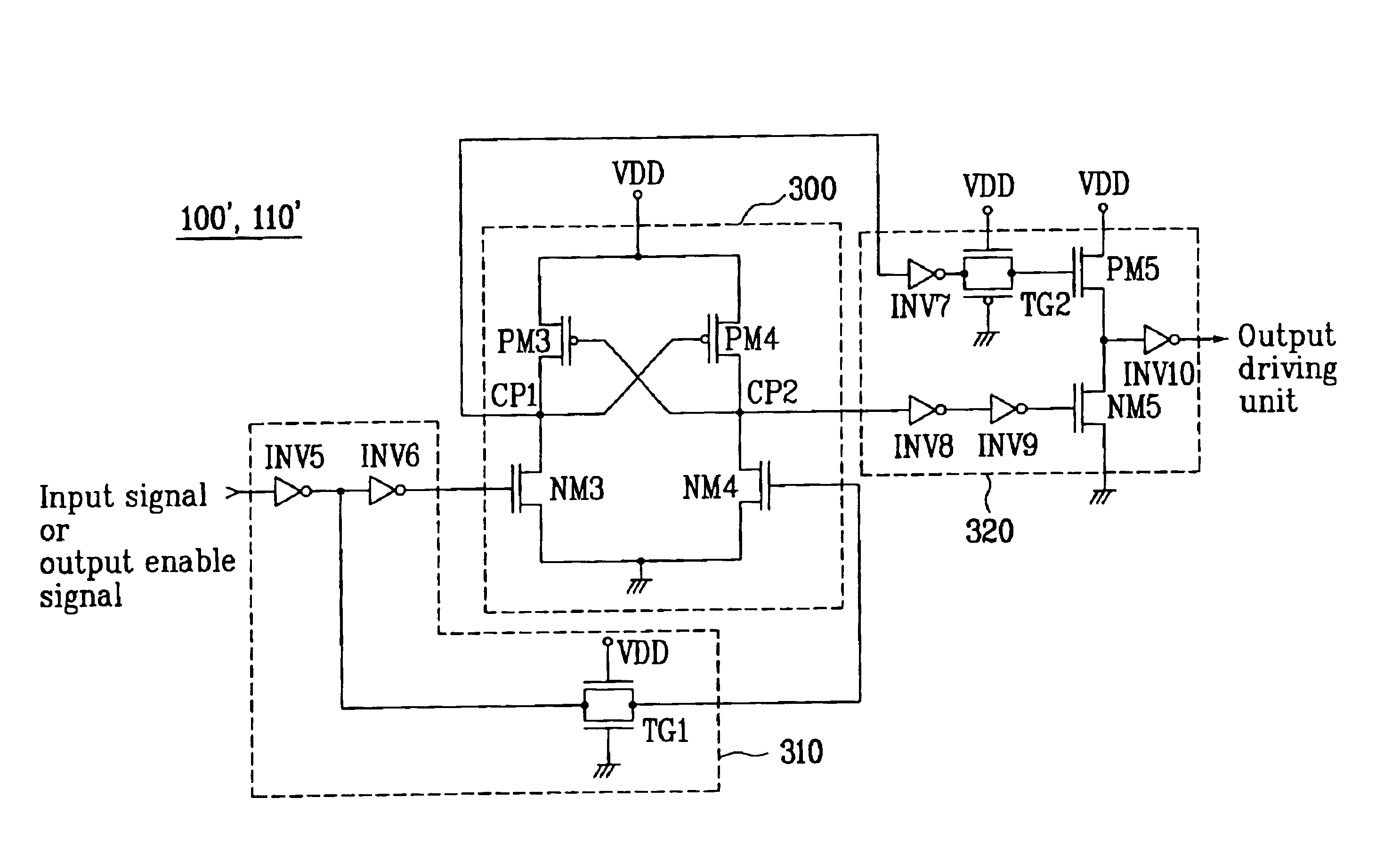
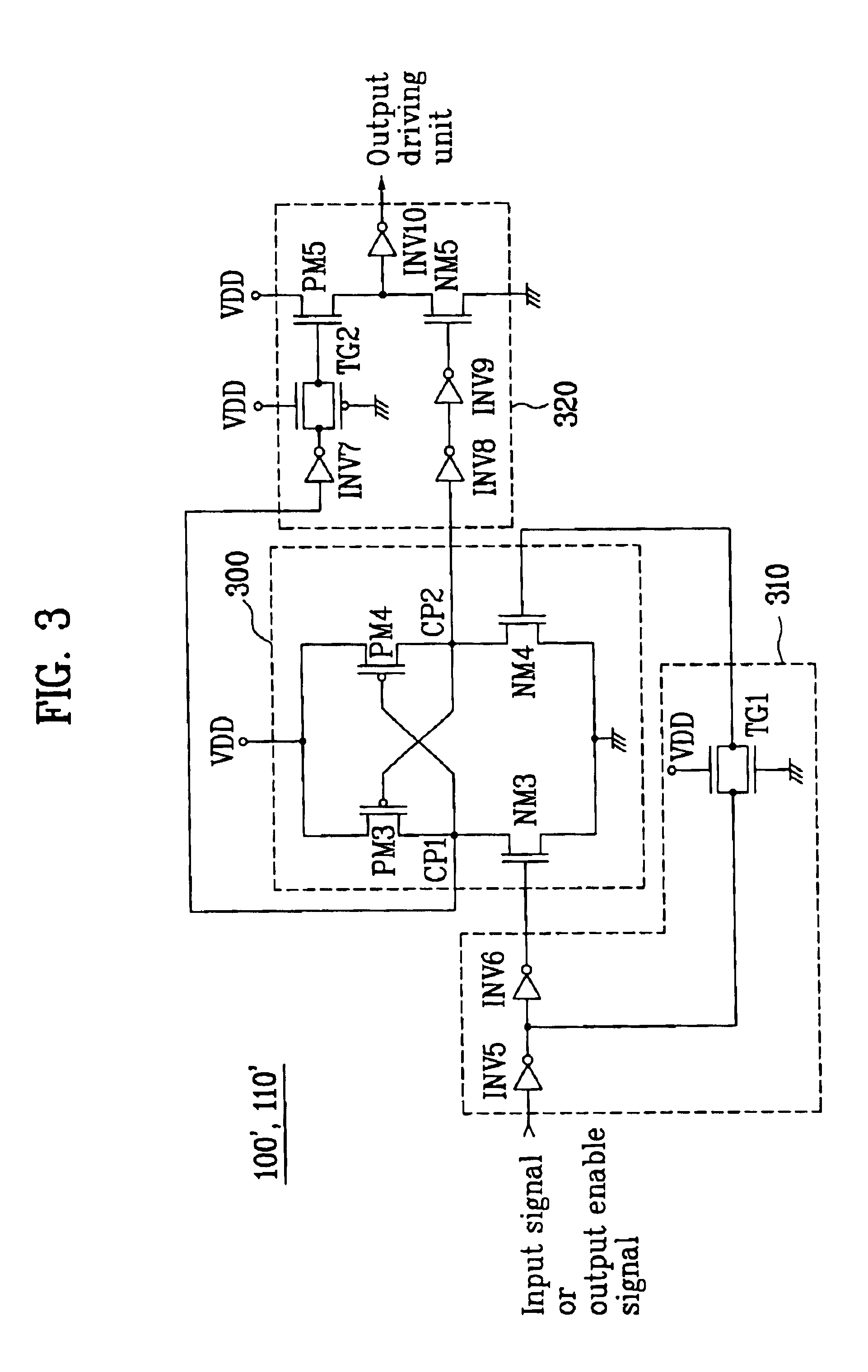
[0046]FIG. 3 illustrates a circuit diagram of a level shifter in accordance with a first preferred embodiment of the present invention.

[0047]Referring to FIG. 3, the level shifter 100′ or 110′ includes an input signal splitting unit 310 for maintaining a delay time period of a received signal constant, a sense amplifier 300 for amplifying the delayed signal, and a delay compensating unit 320.

[0048]The input signal splitting unit 310 includes a plurality of inverters INV5, and INV6, and a transmission gate TG1, wherein the input signal passes through, and is delayed at, the plurality of inverters INV5 and INV6 in succession for a time period, and is provided to the input terminal at one side of the sense amplifier 300, and an output signal from the inverter INV5 is delayed at the transmission gate TG1 for a time period the same with a delay time period at the inverter INV6, and provided to the other side input terminal of the sense amplifier 300.

[0049]The sense amp...

second embodiment

2) Second Embodiment

[0066]FIG. 4 illustrates a circuit diagram of a level shifter in accordance with a second preferred embodiment of the present invention.

[0067]Referring to FIG. 4, the level shifter 100″ or 110″ includes an inverter INV11, a transmission gate TG3, third and fourth level shifters 400 and 410 each for boosting a voltage level of a signal from the inverter INV11 or the transmission gate TG3 to a voltage level of a power terminal VDD, first and second pulse signal generating units 420 and 430 each for generating a pulse signal at a rising edge of the signal from the third or the fourth level shifter 400 or 410, and an output signal generating unit 440 for delaying the signals from the first and second pulse signal generating units 420 and 430 for the same time periods, and generating a signal having a high level voltage and a low level voltage shifted according to the pulse signals the first and second pulse signal generating parts 420 and 430 generate respectively.

[0...


PUM


Abstract

Output driving circuit including at least one or more than one level shifter for receiving an input signal to be provided to an outside of an integrated circuit and shifting a voltage level of the input signal to a voltage level required at the outside of the integrated circuit while maintaining a duty ratio of the input signal constant, and an output driving unit for forwarding the input signal to the outside of the integrated circuit under the control of an output enable signal, thereby permitting application to the integrated circuit operative at a high speed, readily.

Description

[0001]This application claims the benefit of the Korean Application Nos. P2002-67696, and P2002-67697, both filed on Nov. 04, 2002, which are hereby incorporated by reference.BACKGROUND OF THE INVENTION[0002]1. Field of the Invention[0003]The present invention relates to output driving circuits, and more particularly, to an output driving circuit for maintaining duty ratios of input / output signals constant.[0004]2. Background of the Related Art[0005]In general, a core voltage of an integrated circuit differs from an I / O voltage outside of the integrated circuit. Owing to development of technology for reducing power consumption, when the core voltage drops gradually, the outside (PCB board) power of the integrated circuit is maintained without any change. Therefore, for providing a core voltage signal to an outside of the integrated circuit, the output driving circuit is required for shifting a level of the core voltage to a voltage level outside of the integrated circuit.[0006]The o...

Claims


Application Information

Patent Timeline
IPC IPC(8): G11C7/10H03K19/003H03K19/0185
CPCG11C7/1051G11C7/1057H03K19/00323H03K19/018521
Inventor HONG, KUK TAEYI, SEUNG HYUN
Owner LG ELECTRONICS INC
Why Eureka
Try Eureka