Method of forming electronic dies wherein each die has a layer of solid diamond

a technology of electronic dies and diamonds, which is applied in the direction of semiconductor devices, electrical equipment, semiconductor/solid-state device details, etc., and can solve problems such as its destruction

Inactive Publication Date: 2005-08-30
INTEL CORP
View PDF10 Cites 19 Cited by
  • Summary
  • Abstract
  • Description
  • Claims
  • Application Information

AI Technical Summary

Problems solved by technology

Operation of the integrated circuit causes heating thereof and an increase of temperature of the integrated circuit may cause its destruction.

Method used


Image

  • Method of forming electronic dies wherein each die has a layer of solid diamond
  • Method of forming electronic dies wherein each die has a layer of solid diamond
  • Method of forming electronic dies wherein each die has a layer of solid diamond

Examples


Embodiment Construction

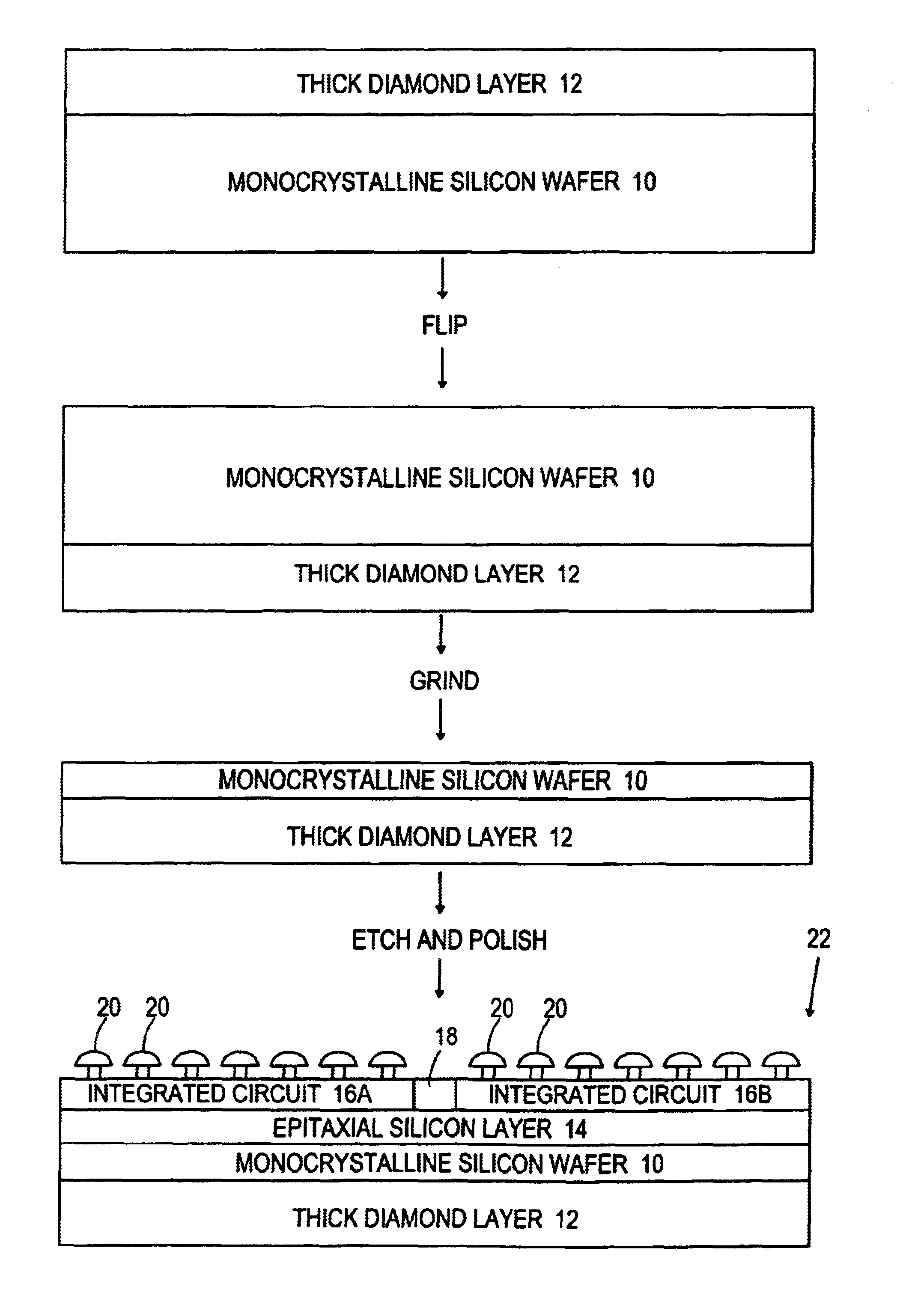
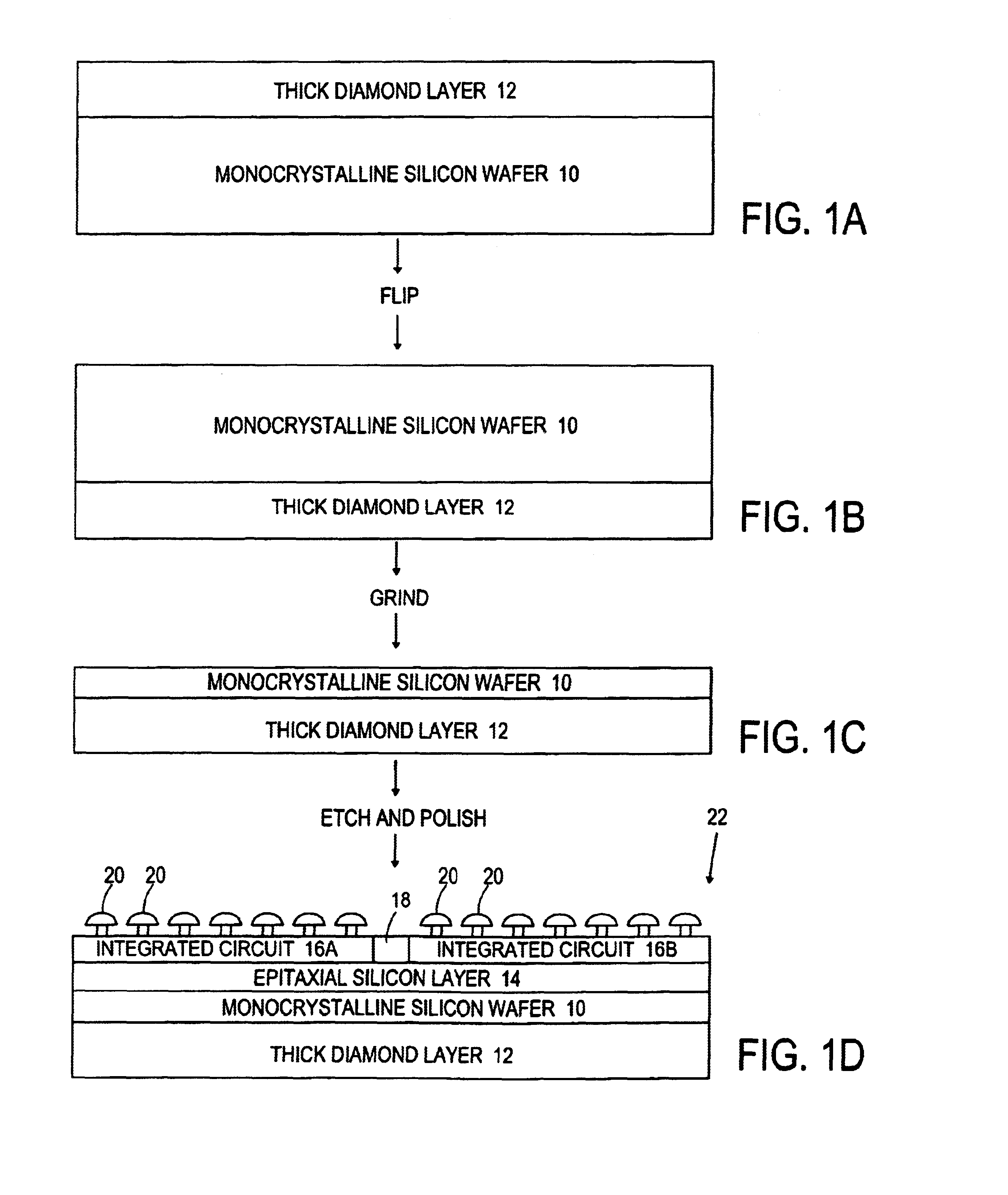
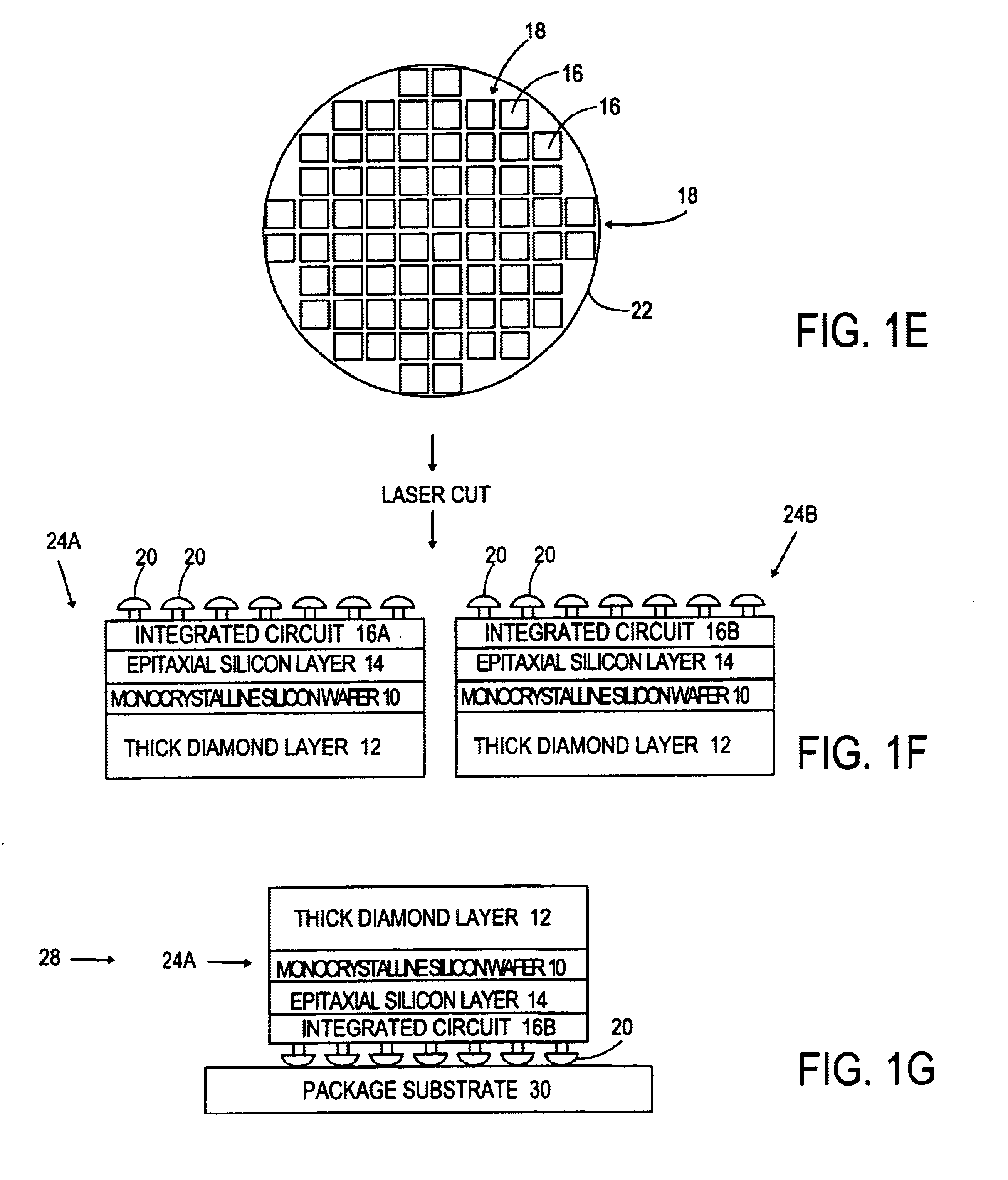
[0043]First, second, and third processes are described respectively with respect to FIGS. 1a-g, FIGS. 2a-h, and FIGS. 3a-j whereby, in each case, a wafer is manufactured, a die from the wafer, and an electronic assembly including the die. The die has a diamond layer which primarily serves to spread heat from hot spots of an integrated circuit in the die.

[0044]In the first process, a relatively thick layer is formed which spreads more heat. The first process however utilizes a relatively cumbersome grinding operation. Because the diamond layer is relatively thick, a specialized laser cutting operation is utilized for cutting through the diamond layer.

[0045]In the second process, the grinding operation of the first process is eliminated and a shearing operation is utilized instead. A thick diamond layer is also formed in the second process, with associated advantages and disadvantages.

[0046]In the third process a shearing operation is also used to eliminate a grinding operation, but a...


PUM

PropertyMeasurementUnit
thickaaaaaaaaaa
thickaaaaaaaaaa
heightaaaaaaaaaa

Abstract

A process is described whereby a wafer is manufactured, a die from the wafer, and an electronic assembly including the die. A thin diamond layer is formed on a sacrificial wafer, and an integrated circuit is then formed on the thin diamond layer. The sacrificial wafer is then removed to expose the thin diamond layer. The resulting combination wafer is subsequently diced into individual dies. Each die has an exposed diamond layer forming the majority of the die and serving to conduct heat from the integrated circuit to a backside of the die, from where the heat can convect or be conducted away from the die.

Description

BACKGROUND OF THE INVENTION[0001]1). Field of the Invention[0002]This invention relates to a method of manufacturing a combination wafer, dies from the wafer, and an electronic assembly including such a die, wherein the die has a layer of diamond for purposes of conducting heat.[0003]2). Discussion of Related Art[0004]Integrated circuits are usually formed on silicon wafers which are subsequently sawed into individual dies. Each die then has a portion of the silicon wafer with a respective integrated circuit formed thereon. Electronic signals can be provided to and from the integrated circuit. Operation of the integrated circuit causes heating thereof and an increase of temperature of the integrated circuit may cause its destruction. The heat usually conducts from the integrated circuit through the portion of the silicon wafer through a backside of the die. Silicon has traditionally been preferred because, in the case of monocrystalline silicon, it is possible to manufacture transis...

Claims


Application Information

Patent Timeline
Patent Type & Authority Patents(United States)
IPC IPC(8): H01L21/70H01L21/02H01L21/30H01L21/301H01L21/00H01L21/46H01L21/78H01L21/68H01L23/373H01L25/065H01L29/16
CPCH01L21/6835H01L23/3732H01L25/0657H01L29/1602H01L24/27H01L2221/68359H01L2224/16H01L2224/274H01L2225/06589H01L2924/16152H01L2924/19041Y10S148/012Y10S438/977H01L2924/3512H01L2924/00H01L2924/10253H01L2924/12042H01L2924/14
Inventor RAVI, KRAMADHATI V.CHRYSLER, GREGORY M.
Owner INTEL CORP
Why Eureka
Try Eureka