

Susceptor for supporting a semiconductor wafer and method for depositing a layer on a front side of a semiconductor wafer
a semiconductor wafer and support technology, applied in the direction of chemically reactive gases, coatings, crystal growth processes, etc., can solve the problems of disrupting the further processing of the semiconductor wafer to form electronic components, and affecting the flatness of the coated semiconductor wafer
Inactive Publication Date: 2012-10-25
SILTRONIC AG
View PDF24 Cites 134 Cited by
- Summary
- Abstract
- Description
- Claims
- Application Information
AI Technical Summary
Problems solved by technology
When an attempt is made to implement this endeavor, a problem encountered is that during deposition of the layer on the front side of the semiconductor wafer, process gas also passes into the edge region of the rear side of the semiconductor wafer.
This results in uncontrolled material deposition in this region, which adversely affects the flatness of the coated semiconductor wafer.
The bump thus adversely affects the fl
Method used
View moreImage
Smart ImageViewing Examples

Examples
 PUM
| Property | Measurement | Unit |
|---|---|---|
| Fraction | aaaaa | aaaaa |
| Area | aaaaa | aaaaa |
Abstract
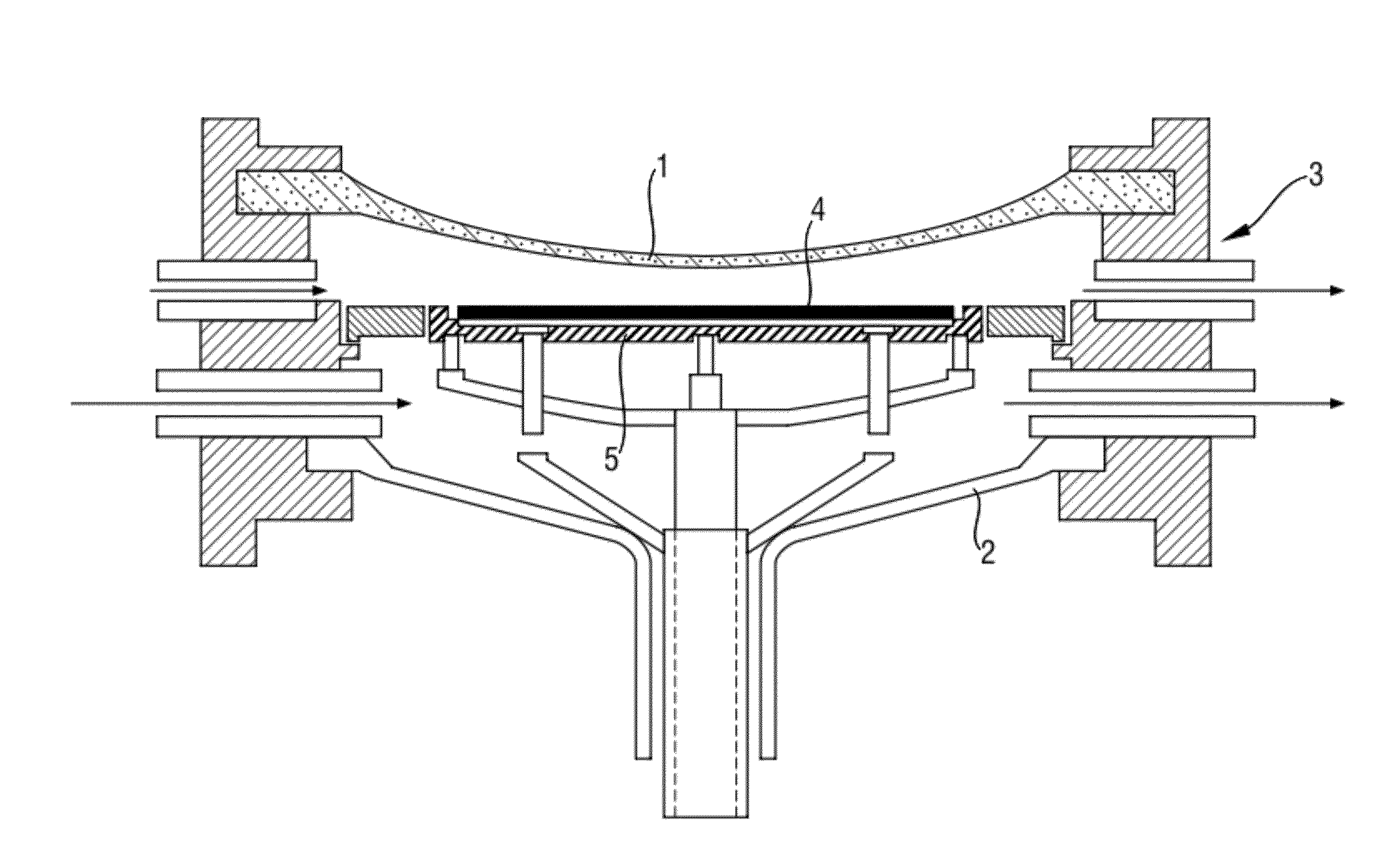
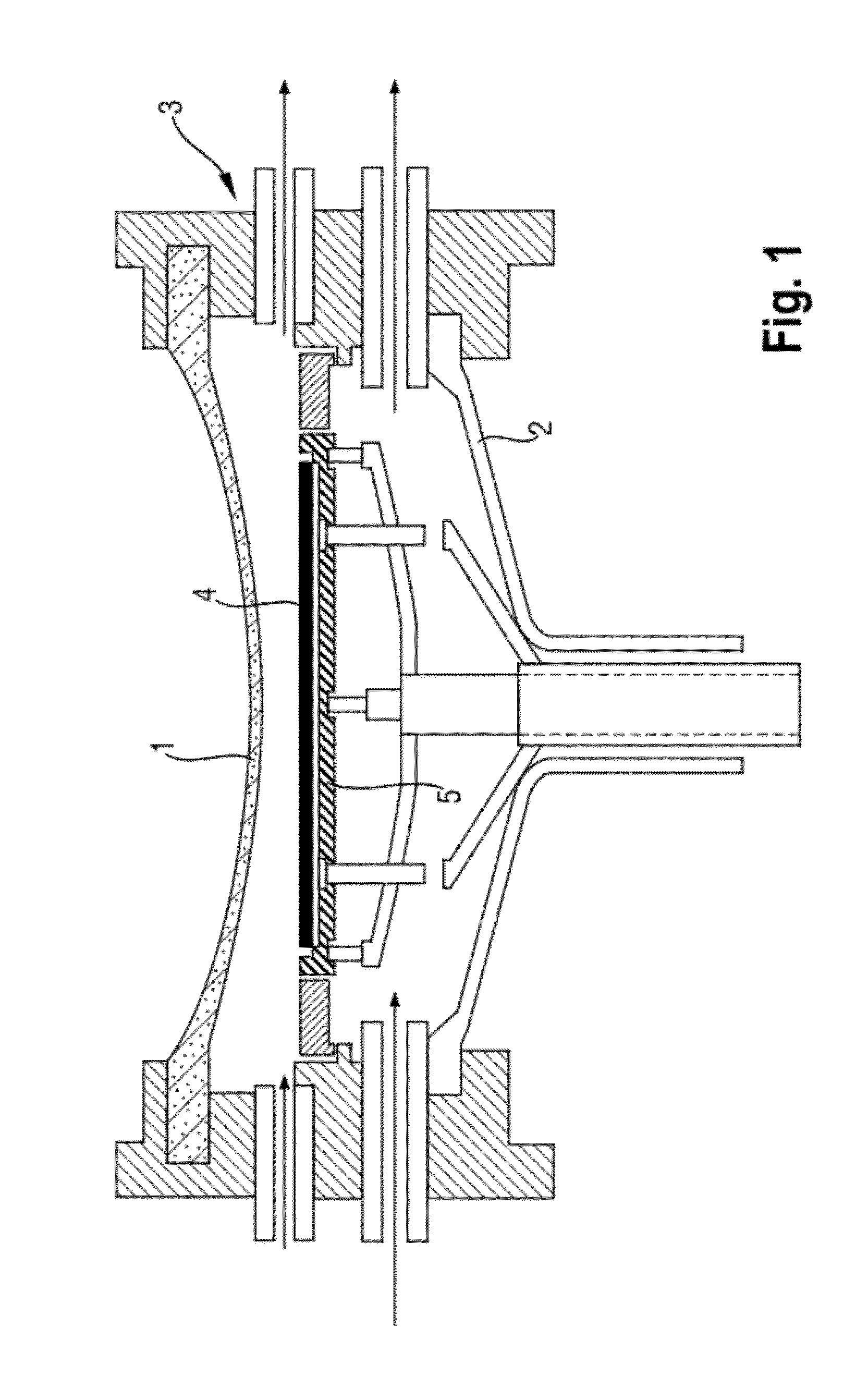
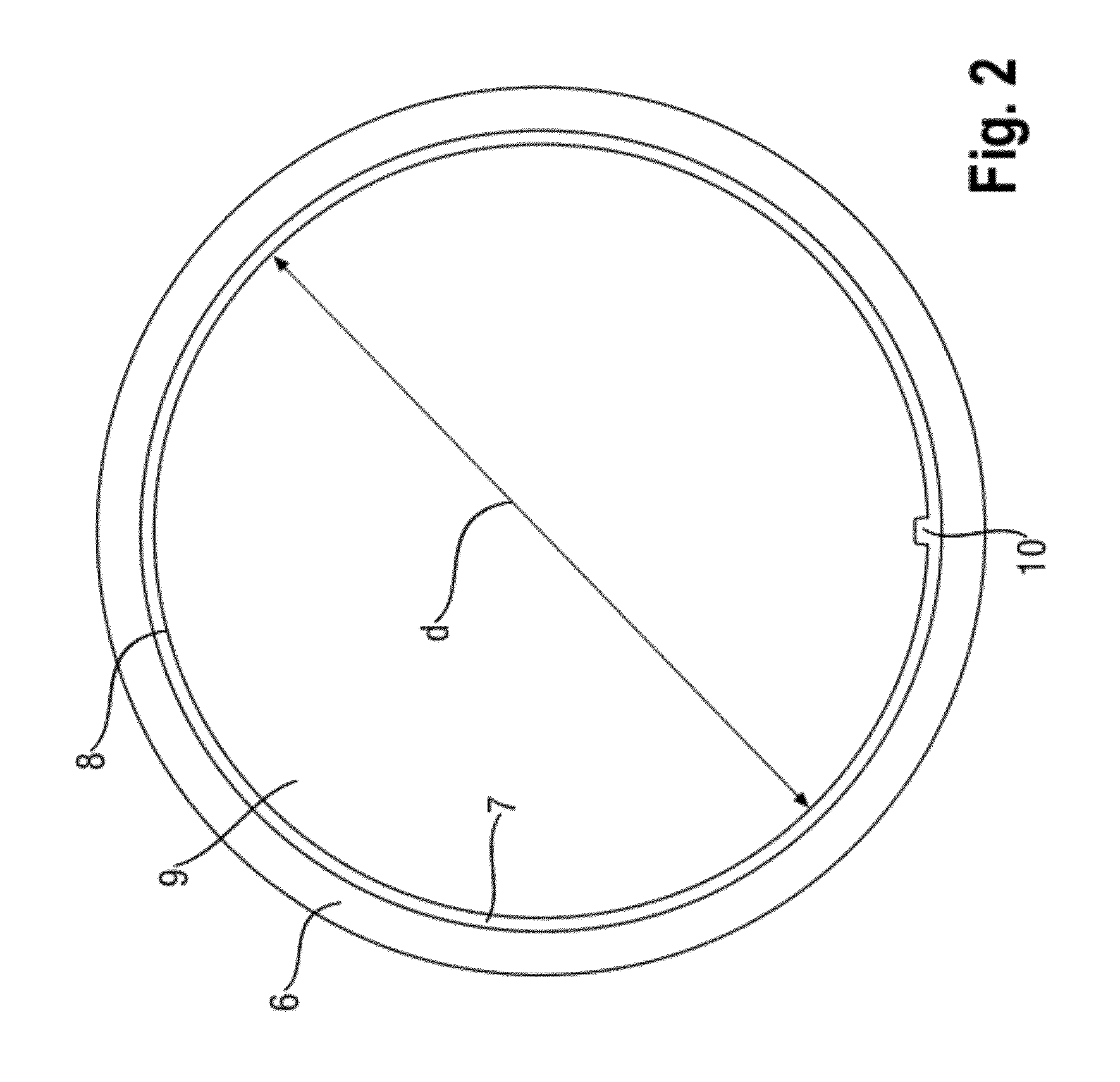
A susceptor for supporting a semiconductor wafer during deposition of a layer on a front side of the semiconductor wafer, the semiconductor wafer having a diameter D and, at its edge, a notch having a depth T, comprising:
- a ring-shaped placement area having an internal diameter d for the placement of the semiconductor wafer in the edge region of a rear side of the semiconductor wafer, wherein, with the semiconductor wafer having been placed, the relationship (D−d)/2<T is satisfied; and
- a protrusion of the area for the placement of semiconductor wafer in the region of the notch of the semiconductor wafer extending the placement area inward, and which completely underlays the notch of the semiconductor wafer.
Description
CROSS-REFERENCE TO RELATED APPLICATIONS[0001]This application claims priority to German Patent Application No. DE 10 2011 007 682.4 filed Apr. 19, 2011 which is herein incorporated by reference.BACKGROUND OF THE INVENTION[0002]1. Field of the Invention[0003]The invention relates to a susceptor for supporting a semiconductor wafer during deposition of a layer on a front side of the semiconductor wafer, wherein the susceptor has a placement area for the placement of the semiconductor wafer in an edge region of the rear side of the semiconductor wafer. The invention also relates to a method for depositing a layer on a front side of a semiconductor wafer, the susceptor being used in this method.[0004]2. Background Art[0005]Susceptors are known in various embodiments. DE 198 47 101 C1 describes an embodiment wherein the placement area is part of a ring that forms the susceptor. In the embodiment of EP 1 460 679 A1 the susceptor additionally has a base and, as a result, the form of a plat...
Claims
Login to View More Application Information
Patent Timeline
 IPC IPC(8): H01L21/02C23C16/458
CPCH01L21/68735C30B25/12C23C16/4585
InventorWERNER, NORBERTHAGER, CHRISTIANSCHAUER, REINHARD
OwnerSILTRONIC AG