

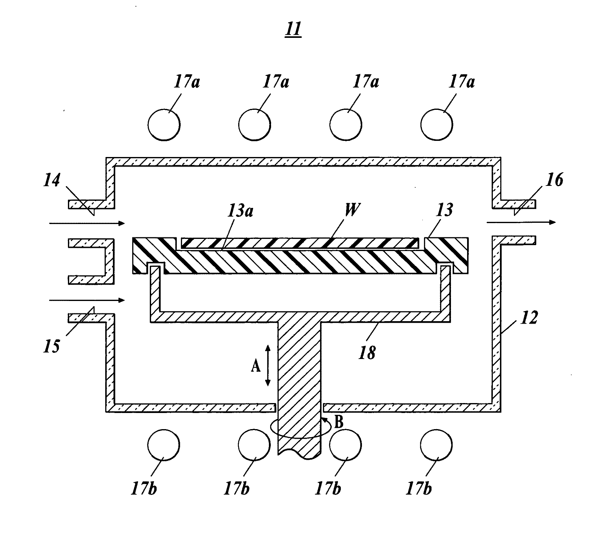
Susceptor and method for manufacturing silicon epitaxial wafer
a technology of susceptor and silicon substrate, which is applied in the direction of polycrystalline material growth, crystal growth process, chemically reactive gas, etc., can solve the problem that document 3 cannot prevent the occurrence of defects, and achieve the effect of preventing warping and slippage of silicon substrate, adhesion of silicon substrate to susceptor, and preventing defects
- Summary
- Abstract
- Description
- Claims
- Application Information
AI Technical Summary
Benefits of technology
Problems solved by technology
Method used
Image

Examples
examples
[0046]Hereinafter, the present invention is described more specifically by giving inventive examples and comparative examples.
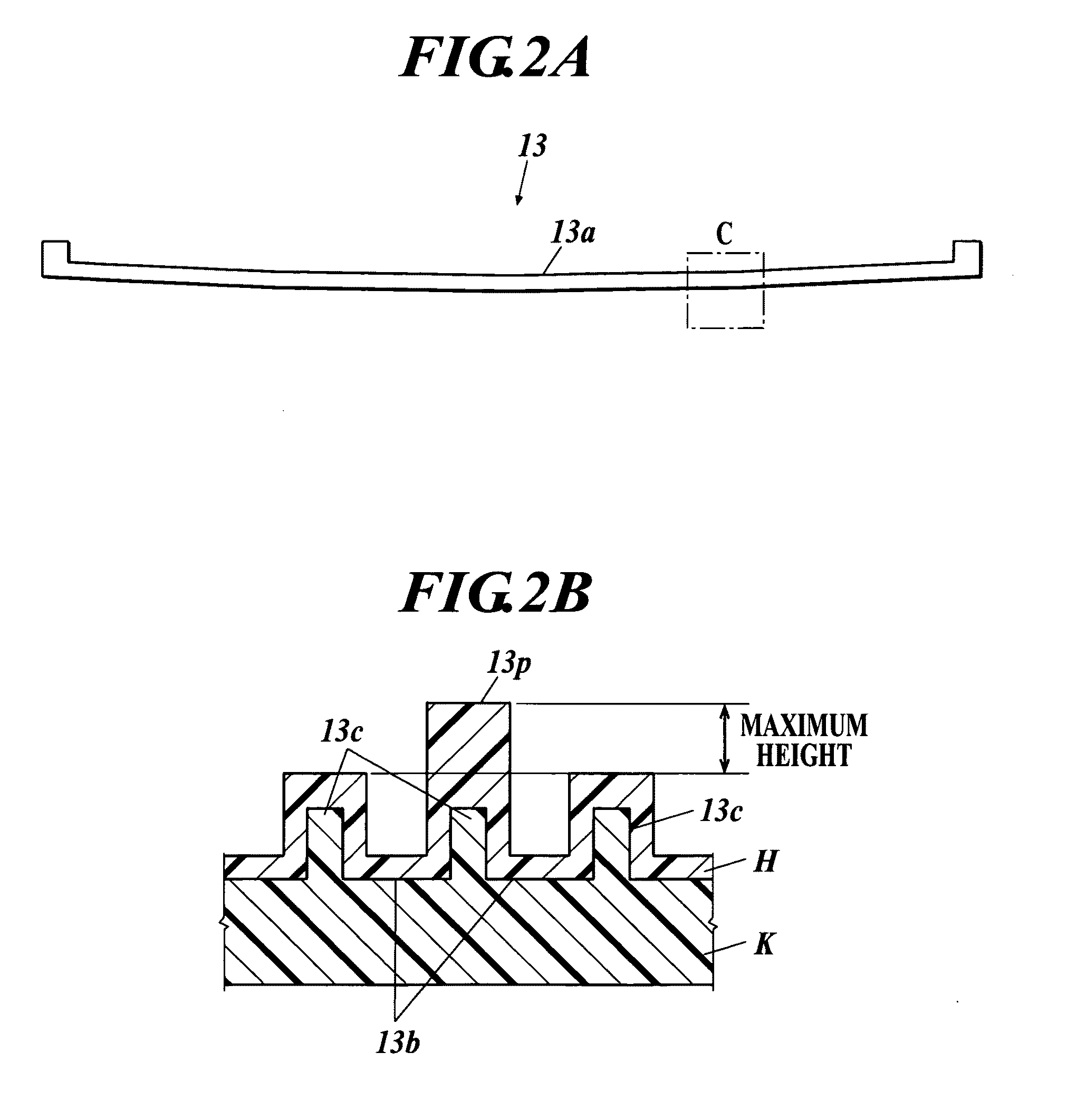
[0047]Susceptors A to H shown in the following Table 1 were prepared as the susceptor 13 of the present embodiment, and epitaxial wafers were produced with these susceptors.
TABLE 1MAXIMUMPROTRUSION HEIGHTSURFACE ROUGHNESS RaSUSCEPTORPOLISH CONDITIONμmμmCOMPARATIVESUSCEPTOR AONLY PROTRUSION POLISH22 1.2 TO 3.1 INCLUSIVEEXAMPLESUSCEPTOR BPROTRUSION POLISH PLUS36 1.1 TO 3.8 INCLUSIVEDISCREET SURFACE POLISHEXAMPLESUSCEPTOR CSAME MATERIALLESS THAN 5 1.0 TO 5.0 INCLUSIVEABRASIVE POLISHSUSCEPTOR DSAME MATERIALLESS THAN 5 1.0 TO 3.0 INCLUSIVEABRASIVE POLISHCOMPARATIVESUSCEPTOR EMAXIMUM POLISHLESS THAN 50.43 TO 0.78 INCLUSIVEEXAMPLESUSCEPTOR FONLY FINISHING POLISHLESS THAN 50.65 TO 0.90 INCLUSIVESUSCEPTOR GROUGH GRIND →LESS THAN 50.11 TO 0.17 INCLUSIVEFINISHING POLISHSUSCEPTOR HROUGH GRIND →LESS THAN 50.11 TO 0.17 INCLUSIVEFINISHING POLISH
[0048]In the present examples...
PUM
| Property | Measurement | Unit |
|---|---|---|
| height | aaaaa | aaaaa |
| roughness | aaaaa | aaaaa |
| roughness | aaaaa | aaaaa |
Abstract
Description
Claims
Application Information