Process for manufacturing photovoltaic cells

a photovoltaic cell and manufacturing technology, applied in the field of photovoltaic cell manufacturing, can solve the problems of high cost of process, aluminum application, etching and replacement process,

Inactive Publication Date: 2005-12-08
BP CORP NORTH AMERICA INC
View PDF6 Cites 177 Cited by
  • Summary
  • Abstract
  • Description
  • Claims
  • Application Information

AI Technical Summary

Problems solved by technology

However, these are not the only methods used to obtain suitable semiconductor wafers for the manufacture of photovoltaic cells.
While such a processing sequence results in an efficient, buried contact photovoltaic cell, the use of hydrochloric acid or other similar etchant to remove the aluminum is not suitable for large-scale commercial production because of the formation of a large amount of spent hydrochloric acid and the slurry of residual aluminum which must be treated in a safe way, and disposed of in an environmentally safe manner.
Additionally, a process where aluminum is applied, etched away and then replaced with a plated metal is an expensive process since it requires the use of a metal layer that is later discarded.

Method used


Image

  • Process for manufacturing photovoltaic cells
  • Process for manufacturing photovoltaic cells

Examples


Embodiment Construction

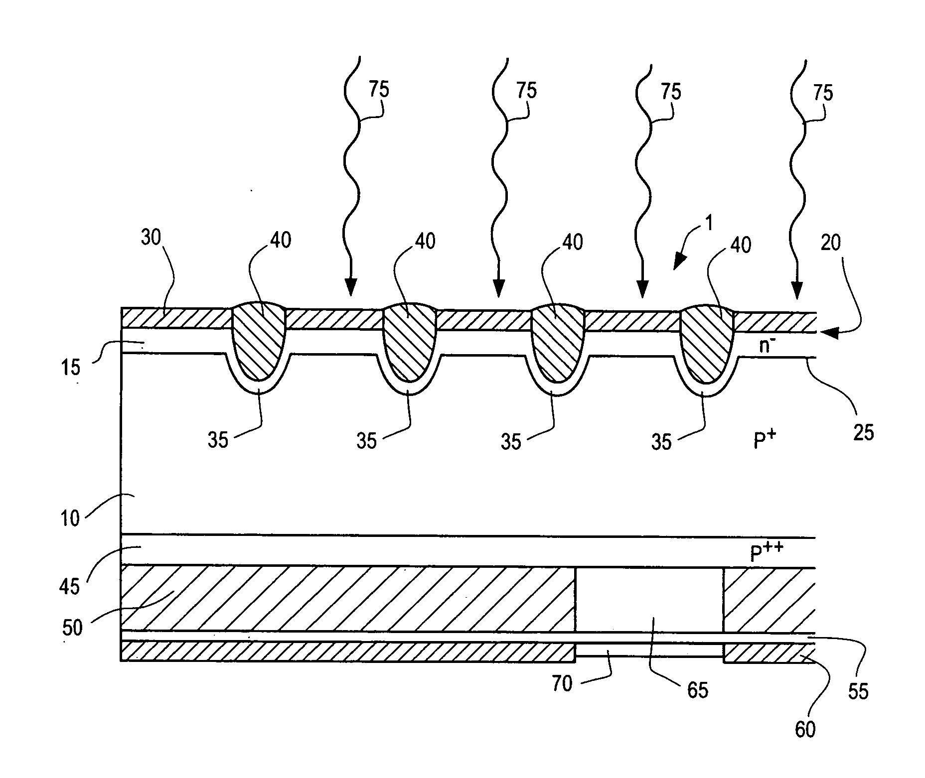
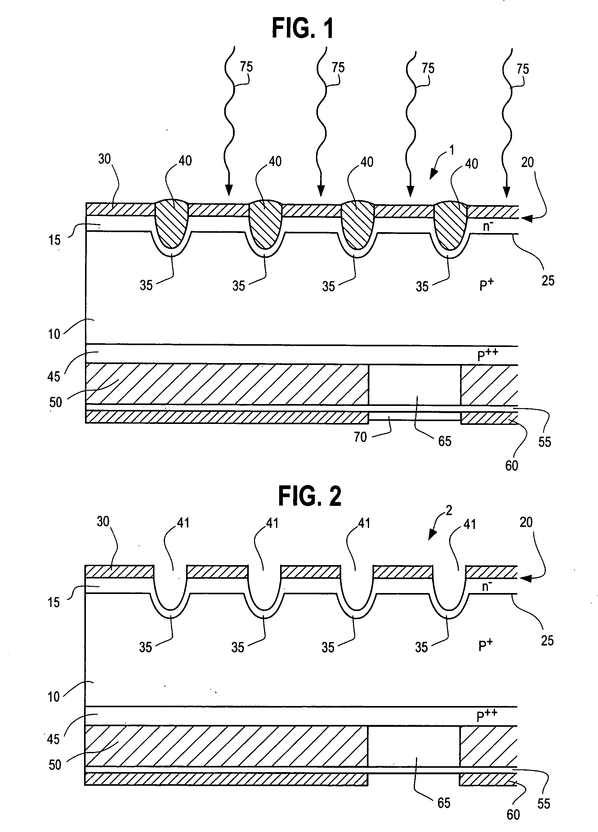
[0020] The invention will now be described using as an example an embodiment of the invention whereby a photovoltaic cell is made using a p-doped silicon wafer. However, it is to be understood that the invention is not limited thereby and is, for example, applicable to other semiconductor materials such as an n-doped silicon wafer.

[0021] A silicon wafer useful in the process of this invention for preparing photovoltaic cells is typically in the form of a thin, flat shape. The silicon may comprise one or more additional materials, such as one or more semiconductor materials, for example germanium, if desired. Although boron is widely used as the first, p-type dopant, other p-type dopants, for example gallium or indium, will also suffice. Boron is the preferred p-type dopant. Combinations of such dopants are also suitable. Thus, the first dopant can comprise, for example, one or more of boron, gallium or indium, and preferably it comprises boron. Suitable wafers are typically obtaine...


PUM

PropertyMeasurementUnit
thickaaaaaaaaaa
thickaaaaaaaaaa
diameteraaaaaaaaaa

Abstract

A process for making a photovoltaic cell using a semiconductor wafer doped with a first dopant, the wafer comprising a front surface and a back surface, the process comprising the steps of forming a first layer on the front surface of the wafer, the first layer comprising a second dopant of a conductivity type opposite the first dopant; depositing a surface coating on the front surface over the first layer; forming grooves in the front surface after depositing the surface coating thereon; adding a second dopant to the grooves; depositing a doping material on the back surface; treating the wafer having the doping material deposited thereon to form a back surface field, masking at least a portion of the back surface of the wafer after the treating; and adding a conductive material to the grooves to form an electrical contact.

Description

[0001] This invention claims the benefit of U.S. Provisional Patent Application No. 60 / 547,123 filed on Feb. 24, 2004.BACKGROUND OF THE INVENTION [0002] This invention relates to a process for manufacturing photovoltaic cells. More particularly, this invention relates to a process for manufacturing photovoltaic cells that are highly efficient in converting light energy, and particularly solar energy, to electrical energy that uses a mask on the back surface of the cell during a plating step in the formation of the electrical contacts for the photovoltaic cell. This invention is also a photovoltaic cell that can be made by such process. [0003] One of the most important features of a photovoltaic cell is its efficiency in converting light energy from the sun into electrical energy. Another important feature is the ability to manufacture such cell in a safe manner applicable to large-scale manufacturing processes. Thus, the art is continuously striving to not only improve the efficienc...

Claims


Application Information

Patent Timeline
Patent Type & Authority Applications(United States)
IPC IPC(8): H01L21/00H01L31/00H01L31/0224H01L31/0352H01L31/068H01L31/18
CPCB23K26/367H01L31/022425Y02E10/547H01L31/068H01L31/03529B23K26/364
Inventor JORDAN, DAVIDWOHLGEMUTH, JOHN H.
Owner BP CORP NORTH AMERICA INC
Why Eureka
Try Eureka