Double-sided N-type crystalline silicon cell and preparation method thereof

A crystalline silicon battery, N-type technology, applied in the direction of circuits, electrical components, photovoltaic power generation, etc., can solve the problems of complicated preparation steps, high cost per watt, and limited price reduction potential, so as to simplify the process flow and reduce surface suspension. Bond density, the effect of reducing the interfacial recombination rate

Inactive Publication Date: 2015-11-11
中国东方电气集团有限公司
View PDF3 Cites 22 Cited by
  • Summary
  • Abstract
  • Description
  • Claims
  • Application Information

AI Technical Summary

Problems solved by technology

At present, commercial high-efficiency cells are all completed on N-type single crystal substrates, typically the back contact cell (IBC) of Sunpower in the United States and the heterojunction cell (HIT) of Sanyo in Japan, with photoelectric conversion efficiencies reaching 24% respectively. % and 22%, but the process involves complicated preparation steps and special equipment, the cost per watt remains high, and the potential for price reduction is limited

Method used


Image

  • Double-sided N-type crystalline silicon cell and preparation method thereof

Examples


Embodiment 1

[0024] A method for preparing a double-sided N-type crystalline silicon solar cell, comprising the steps of:

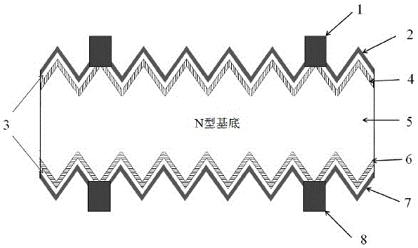
[0025] (1) Using N-type monocrystalline silicon as the substrate, the silicon wafer is cleaned and textured. The resistivity of the N-type monocrystalline silicon substrate is 1~12Ω·cm, and the thickness is 170~200mm;

[0026] (2) Place the above-mentioned silicon chip face-to-face for single-sided boron diffusion. The boron diffusion surface of the silicon chip is the front side, and the sheet resistance is 60Ω / □, using BBr 3 Liquid source diffusion, the diffusion temperature is 970°C, and the time is 50min;

[0027] (3) During the cooling process after the boron diffusion propulsion is completed, a certain flow of oxygen is introduced to oxidize the borosilicate glass and its interface with silicon until the temperature is lowered to 790°C. The flow rate of oxygen is 3-16slm, preferably 5slm, The oxidation time is 3-40min, preferably 20min;

[0028] (4) Deposit a ...

Embodiment 2

[0039] A method for preparing a double-sided N-type crystalline silicon solar cell, comprising the steps of:

[0040] (1) Using N-type monocrystalline silicon as the substrate, the silicon wafer is cleaned and textured. The resistivity of the N-type monocrystalline silicon substrate is 1~12Ω·cm, and the thickness is 170~200mm;

[0041] (2) Place the above-mentioned silicon chip face-to-face for single-sided boron diffusion. The boron diffusion surface of the silicon chip is the front side, and the sheet resistance is 65Ω / □, using BBr 3 Liquid source diffusion, the diffusion temperature is 950°C, and the time is 50min;

[0042] (3) During the cooling process after the boron diffusion propulsion is completed, a certain flow of oxygen is introduced to oxidize the borosilicate glass and its interface with silicon until the temperature is lowered to 790°C. The flow rate of oxygen is 3-16slm, preferably 5slm, The oxidation time is 3-40min, preferably 20min;

[0043] (4) on the bor...

Embodiment 3

[0054] A method for preparing a double-sided N-type crystalline silicon solar cell, comprising the steps of:

[0055] (1) Using N-type monocrystalline silicon as the substrate, the silicon wafer is cleaned and textured. The resistivity of the N-type monocrystalline silicon substrate is 1~12Ω·cm, and the thickness is 170~200mm;

[0056] (2) Place the above-mentioned silicon chip face-to-face for single-sided boron diffusion. The boron diffusion surface of the silicon chip is the front side, and the sheet resistance is 50Ω / □, using BBr 3 Liquid source diffusion, the diffusion temperature is 970°C, and the time is 60min;

[0057] (3) During the cooling process after the boron diffusion propulsion is completed, a certain flow of oxygen is introduced to oxidize the borosilicate glass and its interface with silicon until the temperature is lowered to 790°C. The flow rate of oxygen is 3-16slm, preferably 5slm, The oxidation time is 3-40min, preferably 20min;

[0058] (4) Deposit a ...


PUM


Abstract

The invention discloses a double-sided N-type crystalline silicon cell comprising a front AgAl electrode, a front antireflection film, a boron emitter passivation layer, a boron emitter p+ layer, an N-type silicon wafer, a phosphorus diffusion n+ back surface field layer, a back passivation layer, a back antireflection film, and a back Ag electrode. The front and the back of the cell are textured surfaces, and both sides can receive light and generate electricity. The boron emitter passivation layer and the back passivation layer are prepared at the same time by growing SiO2 layers through thermal oxidation in a low-temperature dry method, which reduces the interface-state density and the rate of interface recombination. A laminated film composed of a borosilicate glass layer and a silicon nitride layer formed in the diffusion process is used as a boron emitter protection layer. Therefore, boron diffusion surface etching and phosphorous diffusion cross contamination caused by chemical solution are prevented effectively, multiple times of etching and mask deposition in the process are reduced, and the technological process is simplified.

Description

technical field [0001] The invention relates to the technical field of solar cell production, in particular to a double-sided N-type monocrystalline silicon cell structure and a preparation method thereof. Background technique [0002] At present, crystalline silicon cells are the mainstream products in the solar cell market, and crystalline silicon solar cells can be divided into P-type crystalline silicon cells and N-type crystalline silicon cells in terms of material and substrate types. Compared with P-type monocrystalline silicon cells, N-type monocrystalline silicon cells have the characteristics of small light-induced attenuation, good resistance to metal impurity pollution, and long minority carrier diffusion length. This is because (1) The light-induced attenuation effect of the P-type cell is caused by the combination of boron and oxygen in the P-type crystalline silicon substrate. There are boron and oxygen in the medium, and using N-type crystalline silicon inst...

Claims


Application Information

Patent Timeline
Patent Type & Authority Applications(China)
IPC IPC(8): H01L31/042H01L31/0236H01L31/0216H01L31/18
CPCH01L31/02167H01L31/0236H01L31/042H01L31/1804Y02E10/547Y02P70/50
Inventor 张中伟张世勇廖亚琴
Owner 中国东方电气集团有限公司
Why Eureka
Try Eureka