Crystalline silicon solar cell capable of realizing double-side light entrance and preparation method therefor

A crystalline silicon solar cell, double-sided light input technology, applied in the field of solar cells, can solve the problems of large-scale production stability, yield to be considered, technology not widely popularized, and high production line price, to increase stability and yield. possibility, production feasibility, well-structured effect

Active Publication Date: 2016-02-10
江西昌大高新能源材料技术有限公司
View PDF5 Cites 26 Cited by
  • Summary
  • Abstract
  • Description
  • Claims
  • Application Information

AI Technical Summary

Problems solved by technology

For example: the performance of the product still needs to be improved, especially in terms of series resistance; the raw material cost of the product is too high, especially indium tin oxide as a transparent conductive oxide material and silver as the main material of the gate line; the price of the entire production line is too high ; The stability and yield rate of mass production still need to be considered; etc.
These problems have led to the fact that the technology has not yet been widely used

Method used


Image

  • Crystalline silicon solar cell capable of realizing double-side light entrance and preparation method therefor

Examples


Embodiment 1

[0027] Taking the n-type single crystal silicon wafer as the base, the present invention will be further described by describing specific implementation cases in combination with the content of the present invention.

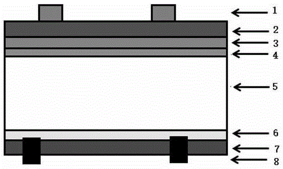
[0028] figure 1 The preparation technology route of the entire device structure shown in , and the material composition of each part are described as follows:

[0029] Step 1: Texturing and cleaning of the crystalline silicon wafer 5 . The double-sided texturing of the silicon wafer is carried out with heated NaOH solution, and the silicon wafer is cleaned with HCl solution after texturing, and then washed with a large amount of deionized water and then dried.

[0030] Step 2: Phosphorous doped crystalline silicon film back electric field layer 6 is prepared by phosphorus oxychloride diffusion method. Silicon wafers are diffused back to back in a high-temperature diffusion furnace; after the diffusion is completed, use nitric acid + hydrofluoric acid solution ...

Embodiment 2

[0039] Taking the n-type single crystal silicon wafer as the base, the present invention will be further described by describing specific implementation cases in combination with the content of the present invention.

[0040] figure 1 The preparation technology route of the entire device structure shown in , and the material composition of each part are described as follows:

[0041] Step 1: Texturing and cleaning of the crystalline silicon wafer 5 . The heated NaOH+surfactant solution is used to make double-sided texture on the silicon wafer. After the texture is made, the silicon wafer is cleaned with HCl solution, and then washed with a large amount of deionized water and then dried.

[0042]Step 2: Phosphorous doped crystalline silicon film back electric field layer 6 is prepared by phosphorus oxychloride diffusion method. Silicon wafers are diffused back to back in a high-temperature diffusion furnace; after the diffusion is completed, use nitric acid + hydrofluoric aci...


PUM

PropertyMeasurementUnit
electrical resistivityaaaaaaaaaa

Abstract

A crystalline silicon solar cell capable of realizing double-side light entrance and a preparation method therefor are disclosed. The crystalline silicon solar cell comprises a metal grid line I, a transparent conductive oxide antireflection conductive layer, a doped silicon based thin film emitting electrode layer, an intrinsic silicon based thin film passivating layer, a crystal silicon wafer, a doped crystalline silicon thin film back surface field layer, a passivating antireflection layer and a metal grid line II. The preparation method comprises the steps of cleaning and texturing firstly, then preparing the doped crystalline silicon thin film back surface field layer, the passivating antireflection layer and the metal grid line II in sequence; then cleaning the surface, of the crystal silicon wafer, where the emitting electrode is positioned, then preparing the intrinsic silicon based thin film passivating layer, the doped silicon based thin film emitting electrode layer, the transparent conductive oxide antireflection conductive layer and the metal grid line I in sequence. The crystalline silicon solar cell has the advantages of capability of realizing double-side light entrance, high open-circuit voltage and good low light effect; the series resistance of the solar cell is further reduced, the consumption of valuable raw materials is reduced, and the cost is reduced; and in addition, the preparation method is suitable for large-scale production, capable of reducing the cost of the production equipment, and is expected to improve the stability and the yield of the products.

Description

technical field [0001] The invention belongs to the technical field of solar cells, and relates to the structure and preparation method of solar cells. Background technique [0002] In the field of solar cells, it is recognized that the solar cell technology that can replace p-type diffused crystalline silicon solar cells and become the mainstream in the market is based on n-type crystalline silicon wafers. The most potential is heterogeneous crystalline silicon solar cell technology. The preparation technology represented by Japan's Panasonic's HIT, which is currently the mainstream technology of this type of solar cell, has the advantages of high open circuit voltage, double-sided light input, good weak light effect, and no PID effect. There are still many problems to be overcome for large-scale popularization. For example: the performance of the product still needs to be improved, especially in terms of series resistance; the raw material cost of the product is too high...

Claims


Application Information

Patent Timeline
Patent Type & Authority Applications(China)
IPC IPC(8): H01L31/068H01L31/0224H01L31/18
CPCH01L31/022425H01L31/068H01L31/1804Y02E10/547Y02P70/50
Inventor 黄海宾周浪
Owner 江西昌大高新能源材料技术有限公司
Why Eureka
Try Eureka