Method and device for protecting micro electromechanical systems structures during dicing of a wafer

Inactive Publication Date: 2002-06-20
ANALOG DEVICES INC
View PDF20 Cites 172 Cited by
  • Summary
  • Abstract
  • Description
  • Claims
  • Application Information

AI Technical Summary

Benefits of technology

0029] A sixth aspect of the present invention is a method for making a protected MEMS structure. The method prepares a MEMS wafer having a plurality of MEMS structure sites thereon; mounts, upon the MEMS wafer, a spacer layer, the spacer layer being perforated in areas corresponding to locations of the MEMS structure sites on the MEMS wafer; and mounts, upon the spacer layer, a wafer cap to produce a laminated MEMS wafer, the spacer layer having a height to prevent electrostatically induced damage to the MEMS wafer.
0030] A seventh aspect of the present invention is a method for making a protected MEMS structure. The method prepares a MEMS wafer having a plurality of MEMS structure sites thereon; mounts, upon the MEMS wafer, a spacer layer, the spacer layer being perforated in areas corresponding to locations of the MEMS structure sites on the MEMS wafer; and mounts, upon the spacer layer, a wafer cap to produce a laminated MEMS wafer, the spacer layer having a height to prevent damage to the MEMS structures due to the wafer cap coming into physical contact with the MEMS wafer.
0031] An eighth aspect of the present invention is a method for making a protected MEMS structure. The method prepares a MEMS wafer having a plurality of MEMS structure sites thereon; mounts, upon the MEMS wafer, a spacer layer, the spacer layer being perforated in areas corresponding to locations of the MEMS structure sites on the MEMS wafer; and mounts, upon the spacer layer, a wafer cap to produce a laminated MEMS wafer, the spacer layer having a height to prevent electrostatically induced damage to the MEMS wafer and to prevent damage to the MEMS structures due to the wafer cap coming into physical contact with the M

Problems solved by technology

However, the micro electromechanical systems structure cannot be passivated since it must be able to move freely.
Due to the fact that the micro electromechanical systems structure is comprised of extremely small sections of polysilicon so that it is resilient, the micro electromechanical systems structure is extremely fragile and great care must be taken during fabrication, up to and including the final packaging steps, not to damage or contaminate the micro electromechanical systems structure.
The water jet sprays used in a sawing process would destroy the micro electromechanical systems structure.
If any of the micro electromechanical systems structures happen to survive the water spray during the sawing operation,

Method used


Image

  • Method and device for protecting micro electromechanical systems structures during dicing of a wafer
  • Method and device for protecting micro electromechanical systems structures during dicing of a wafer
  • Method and device for protecting micro electromechanical systems structures during dicing of a wafer

Examples


fourth embodiment

[0169] the present invention protects a MEMS structure during a dicing of a MEMS wafer to produce individual MEMS dies by preparing a MEMS wafer having a plurality of MEMS structure sites thereon; mounting, upon the MEMS wafer, punched tape, the punched tape having holes in areas corresponding to locations of the MEMS structure sites on the MEMS wafer; mounting, upon the punched tape, a cover tape to produce a laminated MEMS wafer, the cover tape being without openings; and dicing the laminated MEMS wafer into a plurality of MEMS dies.

[0170] The cover tape may include an adhesive medium. The adhesive medium may be an ultraviolet light releasable medium, a heat releasable medium, a combination of an ultraviolet light and heat releasable medium, a thermoplastic organic material, or an ultraviolet light sensitive organic material.

[0171] A contiguous tape may be applied to a backside of the MEMS wafer, the backside of the MEMS wafer being a side opposite of a side having the MEMS struct...

fifth embodiment

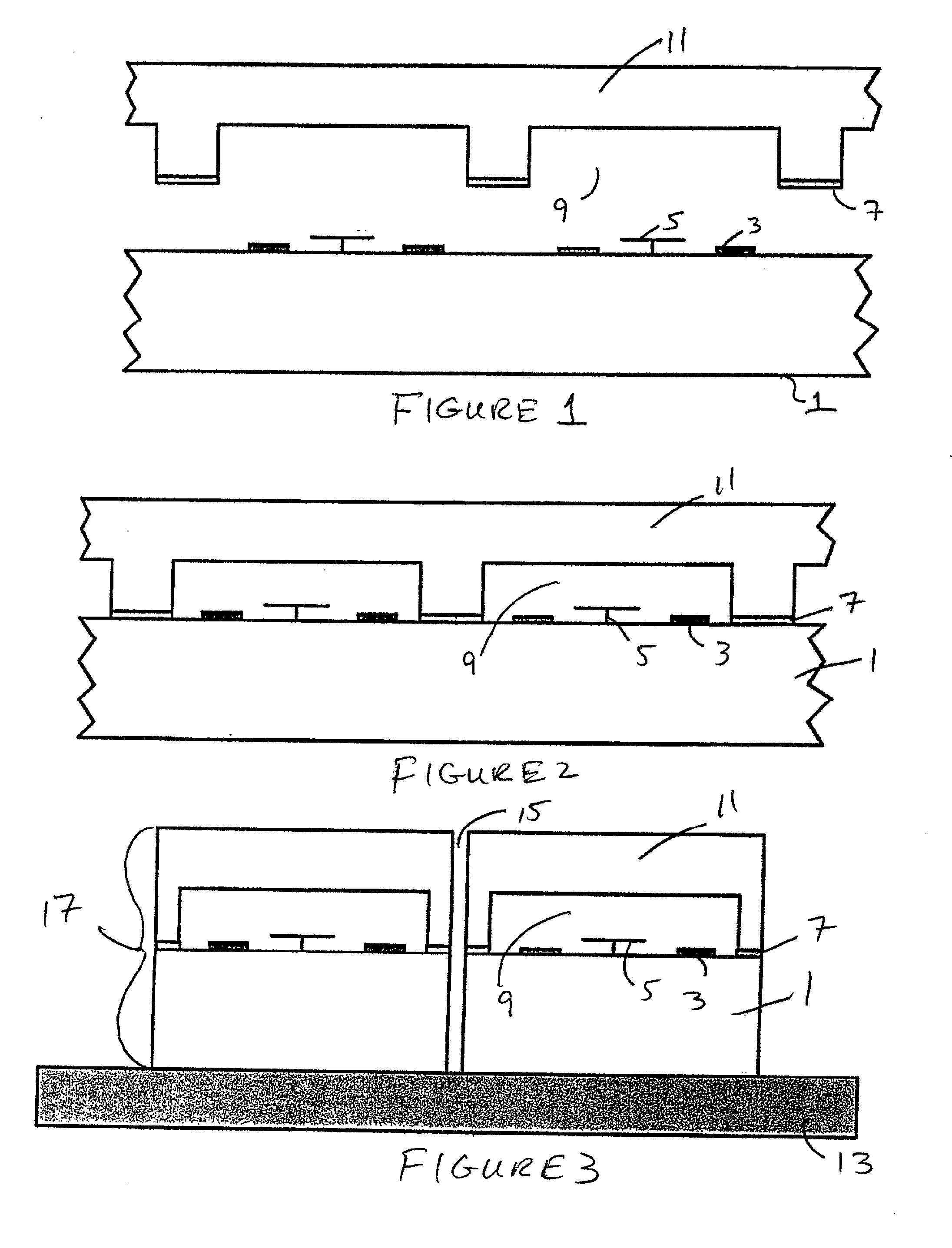
[0173] the present invention makes a protected MEMS structure by preparing a MEMS wafer having a plurality of MEMS structure sites thereon; mounting, upon the MEMS wafer, a spacer layer, the spacer layer being perforated in areas corresponding to locations of the MEMS structure sites on the MEMS wafer; and mounting, upon the spacer layer, a wafer cap to produce a laminated MEMS wafer, the spacer layer having a height to prevent electrostatically induced damage to the MEMS wafer.

[0174] The spacer layer may comprise a tape having adhesive on two sides and a flexible film or a flexible film with an adhesive medium on one side. The flexible film may be transmissive to UV radiation and may be about 40 mils thick. The spacer layer may also comprise a plurality of layers of perforated tape; an aggregate of the plurality of layers of perforated tape producing the height to prevent electrostatically induced damage to the MEMS wafer.

[0175] The wafer cap may be a cover tape wherein the cover t...

sixth embodiment

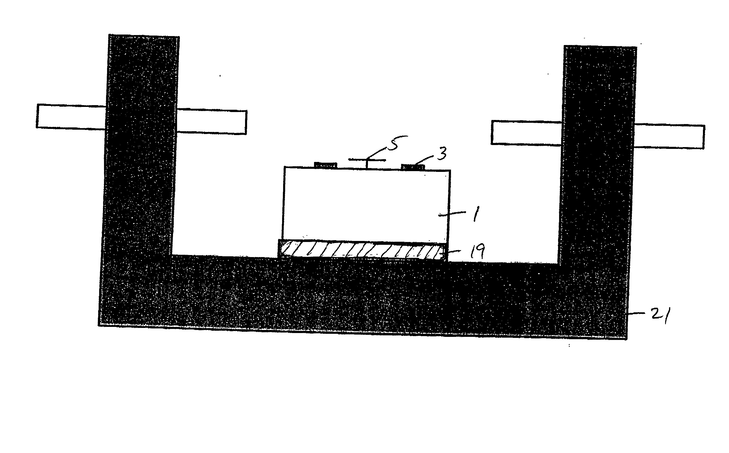
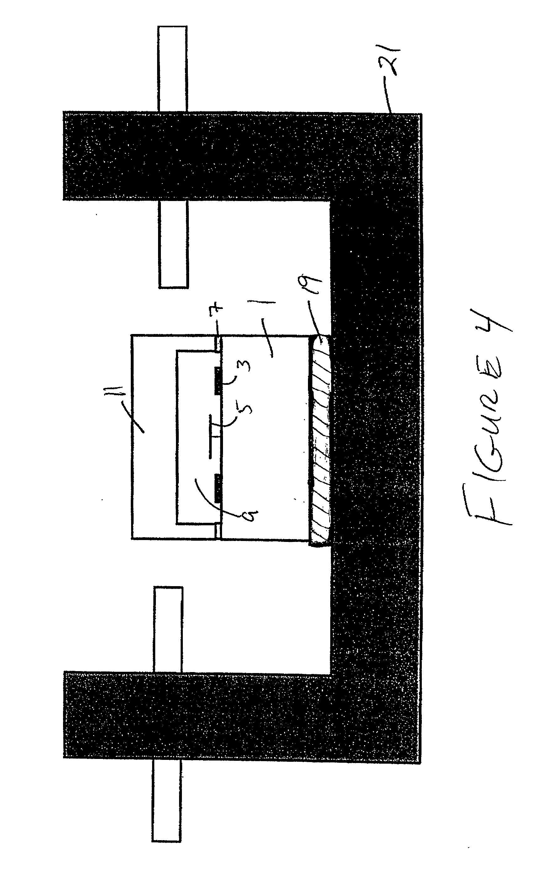
[0178] the present invention makes a protected MEMS structure by preparing a MEMS wafer having a plurality of MEMS structure sites thereon; mounting, upon the MEMS wafer, a spacer layer, the spacer layer being perforated in areas corresponding to locations of the MEMS structure sites on the MEMS wafer; and mounting, upon the spacer layer, a wafer cap to produce a laminated MEMS wafer, the spacer layer having a height to prevent damage to the MEMS structures due to the wafer cap coming into physical contact with the MEMS wafer.

[0179] The spacer layer may comprise a tape having adhesive on two sides and a flexible film or a flexible film with an adhesive medium on one side. The flexible film may be transmissive to UV radiation and may be about 40 mils thick. The spacer layer may also comprise a plurality of layers of perforated tape, an aggregate of the plurality of layers of perforated tape producing the height to prevent the wafer cap from coming into physical contact with the MEMS ...


PUM

PropertyMeasurementUnit
Flexibilityaaaaaaaaaa
Adhesivityaaaaaaaaaa
Areaaaaaaaaaaa

Abstract

A wafer cap protects micro electromechanical system ("MEMS") structures during a dicing of a MEMS wafer to produce individual MEMS dies. A MEMS wafer is prepared having a plurality of MEMS structure sites thereon. Upon the MEMS wafer, the wafer cap is mounted to produce a laminated MEMS wafer. The wafer cap is recessed in areas corresponding to locations of the MEMS structure sites on the MEMS wafer. The capped MEMS wafer can be diced into a plurality of MEMS dies without causing damage to or contaminating the MEMS die.

Description

PRIORITY INFORMATION[0001] This application claims priority from both U.S. Provisional Patent Application, Serial No. 60 / 251,287, filed on Dec. 5, 2000 and U.S. Provisional Patent Application, Serial No. 60 / 251,288, filed on Dec. 5, 2000.FIELD OF THE PRESENT INVENTION[0002] The present invention is directed to protecting micro electromechanical systems ("MEMS") structures during dicing of a MEMS wafer to produce individual MEMS dies. More particularly, the present invention is directed to providing a removable wafer cap that is recessed in areas corresponding to locations of individual MEMS structure sites on the MEMS wafer wherein the MEMS wafer, with wafer cap in place, is diced into a plurality of MEMS dies.BACKGROUND OF THE PRESENT INVENTION[0003] Conventionally, in fabricating MEMS dies for use in the electronics industry, a MEMS wafer is typically fabricated which comprises a plurality of individual MEMS dies commonly arranged in a grid pattern. The sections of a wafer between...

Claims


Application Information

Patent Timeline
IPC IPC(8): B81B7/00B81C1/00H01L21/68
CPCB81C1/00888H01L2221/68327H01L21/6836B81C1/00896
Inventor SPOONER, TIMOTHY R.COURAGE, DAVID S.WORKMAN, BRAD
Owner ANALOG DEVICES INC
Why Eureka
Try Eureka