Wafer level package structure with a heat slug
- Summary
- Abstract
- Description
- Claims
- Application Information
AI Technical Summary
Benefits of technology
Problems solved by technology
Method used
Image
Examples
Embodiment Construction
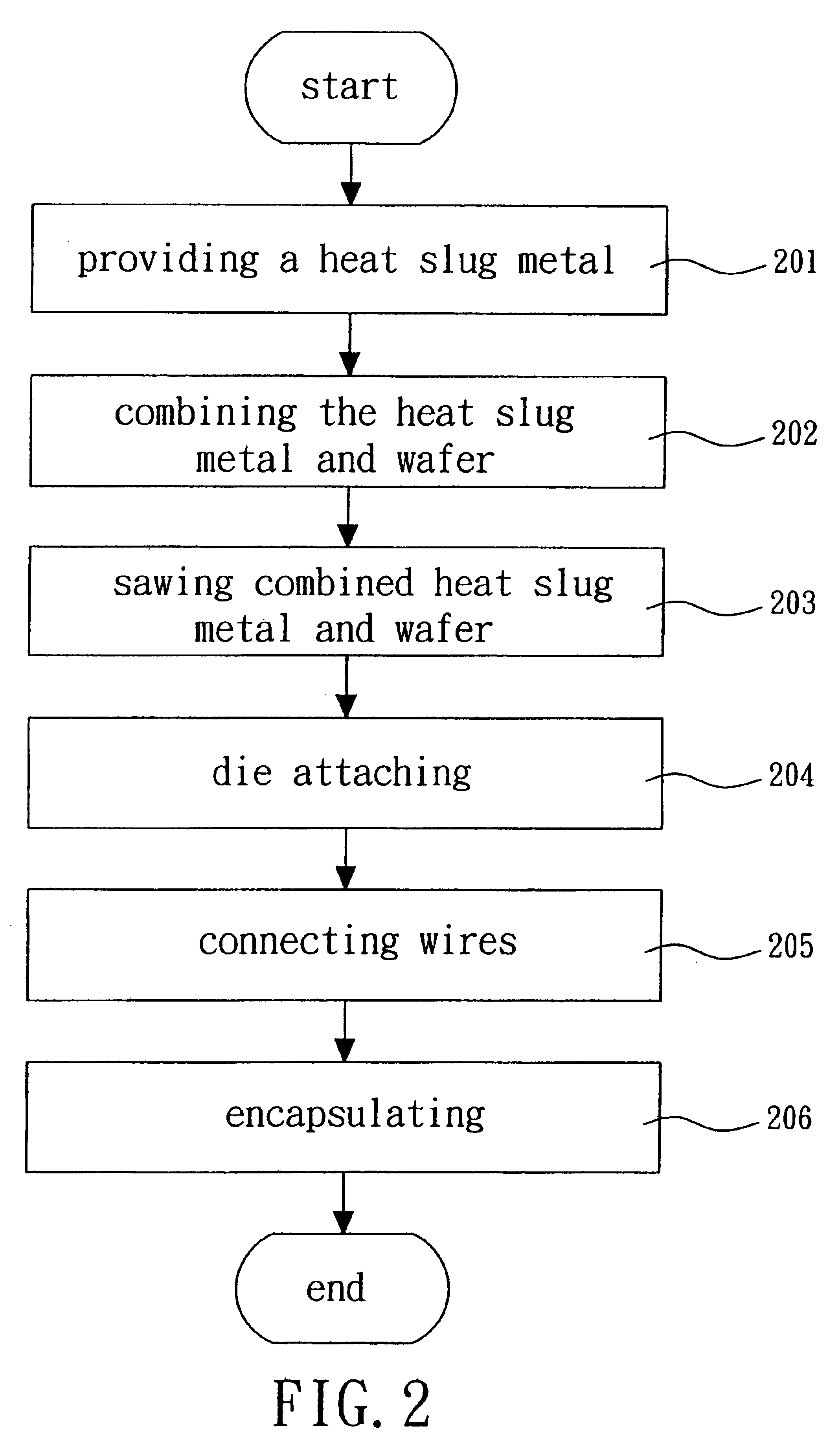
[0020]Referring to FIG. 2, a flow chart of the method for packaging a wafer level package according to the preferred embodiment of present invention is shown. First, in step 201, a heat slug metal 3 as shown in FIG. 3 is provided. The heat slug metal 3 has a plurality of openings 31, 32 thereof The heat slug metal 3 can be designed to be sawed into a plurality of heat slugs 33 (as illustrated in the sawing lines 34, 35, the size is approximately equal to the die.)
[0021]In step 202, the heat slug metal 3 is mounted onto a wafer. The wafer has not been sawed. After the heat slug metal 3 and the wafer are combined, the openings 31, 32 of the heat slug metal 3 are disposed on the position corresponding to the bonding pads of the wafer, and the bonding pads are exposed.
[0022]In step 203, the combined heat slug metal 3 and wafer is sawed into a plurality of die units 4 along the sawing lines 34, 35. In this step, the heat slug metal 3 and wafer are sawed at the same time, so as to improve...
PUM
 Abstract
Description
Claims
Application Information


