Thermal testing method for integrated circuit chips and packages

a technology of integrated circuit chips and packages, which is applied in the direction of semiconductor/solid-state device testing/measurement, semiconductor/solid-state device details, instruments, etc., can solve the problems of affecting the reliability and/or performance of the integrated circuit (ic) chip during operation, causing more heat, and reducing the reliability of the integrated circuit (ic) chip

Active Publication Date: 2005-09-20
TEXAS INSTR INC
View PDF5 Cites 19 Cited by
  • Summary
  • Abstract
  • Description
  • Claims
  • Application Information

AI Technical Summary

Problems solved by technology

Heat dissipation from an integrated circuit (IC) die or chip during operation is typically an important issue, especially as the density of IC devices on a die continues to increase.
Such high-power transistors tend to produce more heat than low-power transistors.
Hence, the reliability and effectiveness of heat dissipation for a packaged IC chip may greatly affect the reliability and / or performance of an IC chip during operation.
Thus, such prior testing methods may not accurately test the heat path between the die 24 and the die pad 26.

Method used


Image

  • Thermal testing method for integrated circuit chips and packages
  • Thermal testing method for integrated circuit chips and packages

Examples


first embodiment

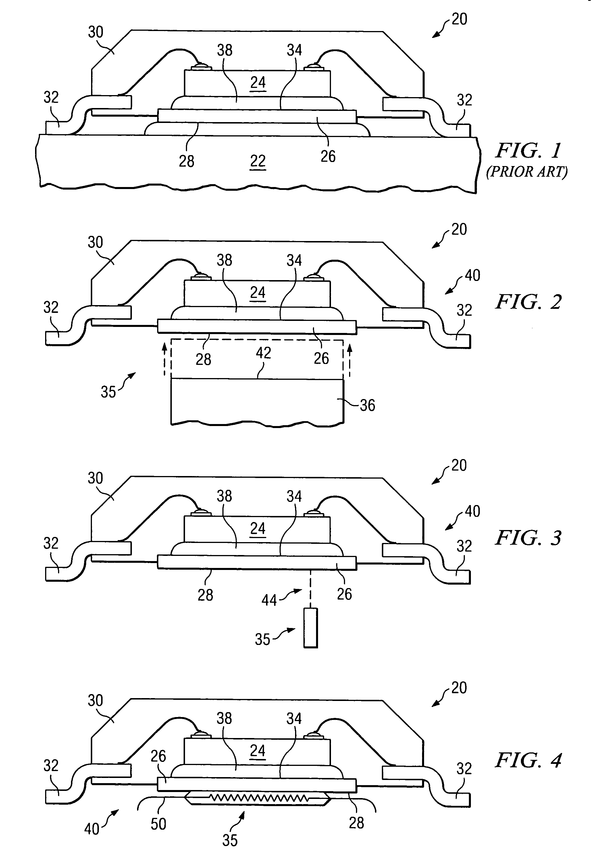
[0024]In the present invention, the external heat source 35 is a heated object 36 or heated mass. As illustrated in FIG. 2, the heat may be applied to the first side 28 of the die pad 26 by touching the heated object 36 to the first side 28 of the die 24. Alternatively, the heated object 36 may not actually touch or physically contact the first side 28 of the die pad26 during a thermal test. It may be sufficient to place the heated object 36 near or proximate to the first side 28 of the die pad 26. Also, it may not be practical or possible to touch the heated object 36 to the first side 28 of the die pad 26 in some cases. As yet another alternative, one or more intermediate materials (not shown) may be placed between the heated object 36 and the first side 28 of the die pad 26. In such case, the heated object 36 may press against the first side of the die pad 26 with the intermediate material(s) located there between.

[0025]The heated object 36 may be made from any of a variety of su...

second embodiment

[0028]In the present invention, a beam 44 of light (e.g., laser) or heat may be projected onto the first side 28 of the die pad 26 for the heating, as illustrated in FIG. 3. The beam 44 of light or heat may have any suitable beam cross-section area. For beam cross-section areas that are much smaller than the die pad 26 (see e.g., FIG. 3), the beam 44 may be moved or scanned about the die pad 26 (in any suitable pattern) for testing the entire die attach interface 38. For some packages, there may be one or a few known locations where delamination is more likely to occur. In such cases, it may be sufficient to test one or a few locations on the die pad 26 to assess the die attachment interface 38. An advantage of using a laser is that the heat may be pulsed or applied intermittently with more precision than applying a heated object 36. Applying heat with a laser or a focused beam of heat also may allow a large temperature differential, relatively quickly. Such heating and rapid change...

third embodiment

[0030]the present invention is illustrated in FIG. 4. In a third embodiment of the present invention, a resistive heating element 50 may be applied to or place near the first side 28 of the die pad 26.

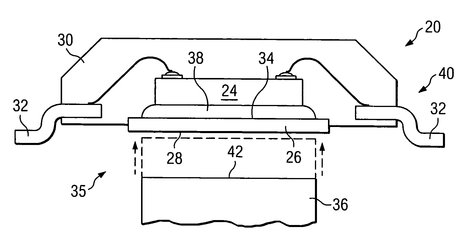
[0031]An embodiment or method of the present invention is advantageous for exposed die pad packages. However, an embodiment or method of the present invention may also be used to thermally test a package (not shown) where the first side 28 of the die pad 26 is not exposed. Hence, a layer of package plastic 30 may be located between the external heat source 35 and the first side 28 of the die pad 26 in such case, for example. However, in such packages where die pad 26 is enclosed in plastic, the primary heat dissipation path is typically through the leads 32. Thus, the external heat source 35 may be applied to the leads 32 rather than the first side 28 of the die pad 26 in such cases to provide a more direct thermal path for testing (as another alternative embodiment).

[0032]Still anothe...


PUM


Abstract

A method of thermally testing for whether an integrated circuit die is attached to a die pad, is provided. Heat is applied from an external heat source to a first side of the die pad. The die is attached to a second side of the die pad. The second side of the die pad is opposite the first side of the die pad. A temperature of the die is measured at a first die location on the die. The die pad is located between the external heat source and the first die location. This method may be performed using a thermal test apparatus having a socket and the external heat source. The socket is adapted to receive and retain one or more leads of a die package. The apparatus may further include a mechanism adapted to move the heat source toward the first side of the die pad.

Description

TECHNICAL FIELD[0001]The present invention relates generally to thermal testing of integrated circuit chips and packages. In one aspect it relates more particularly to thermally testing a die attachment to a die pad or a lead frame.BACKGROUND[0002]Heat dissipation from an integrated circuit (IC) die or chip during operation is typically an important issue, especially as the density of IC devices on a die continues to increase. Also, many devices now have combinations of high-power transistors and low-power transistors formed on a same die. Such high-power transistors tend to produce more heat than low-power transistors. Further, more system-on-chip configurations are being used. Thus, there are often a wide variety of IC devices on a same die. Some of the IC devices can handle and / or put out much more heat than nearby or neighboring devices on the same die. Hence, the reliability and effectiveness of heat dissipation for a packaged IC chip may greatly affect the reliability and / or p...

Claims


Application Information

Patent Timeline
Patent Type & Authority Patents(United States)
IPC IPC(8): G01R31/02H01L21/66H01L23/31
CPCH01L22/10H01L23/3107H01L2224/48091H01L2924/00014H01L2224/32245H01L2224/48247H01L2224/48465H01L2224/73265H01L2924/00H01L2924/3011H01L2924/181H01L2924/00012
Inventor TELLKAMP, JOHN PAUL
Owner TEXAS INSTR INC
Why Eureka
Try Eureka