Padless structure design for easy identification of bridging defects in lines by passive voltage contrast

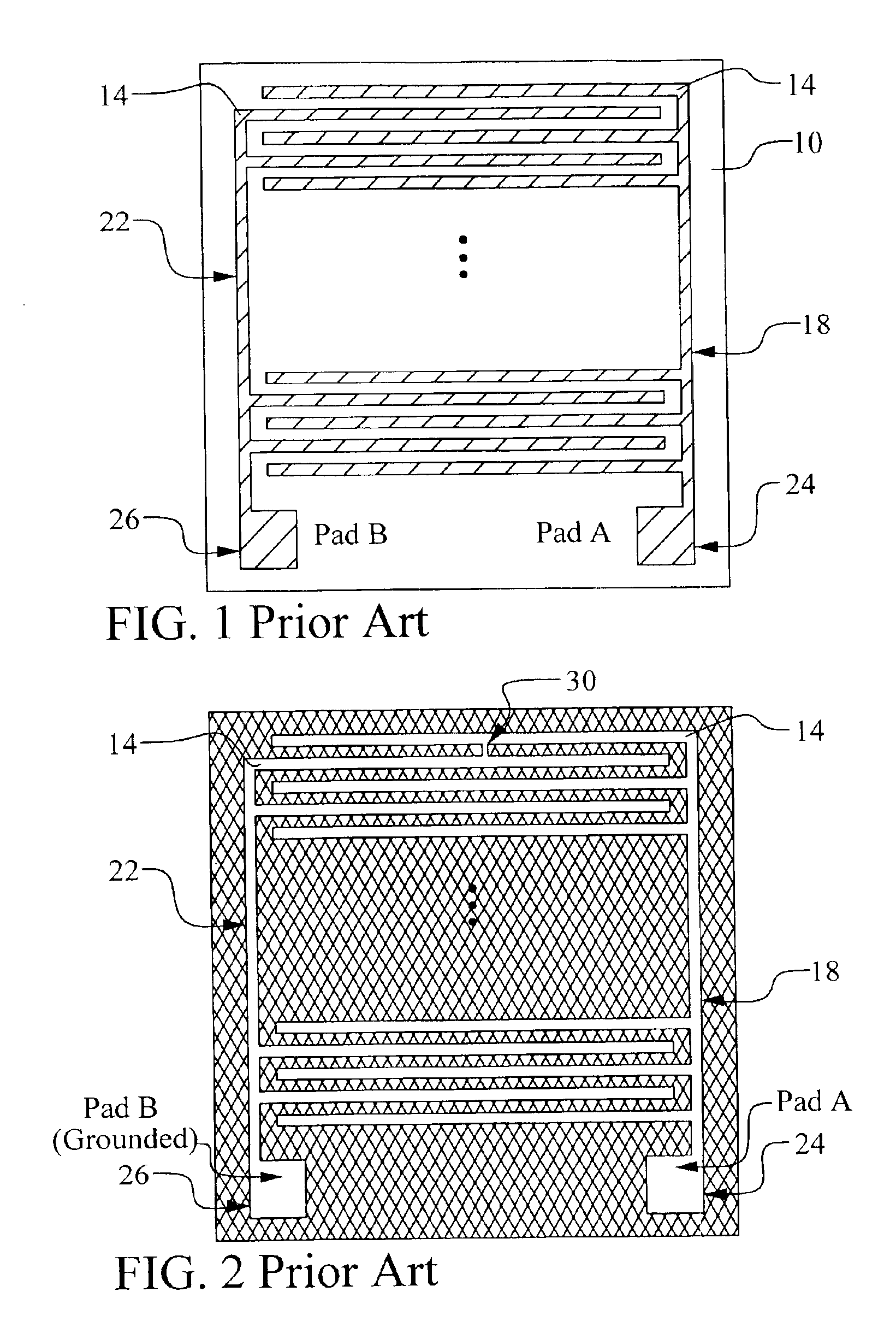
a technology of passive voltage contrast and bridging defect, which is applied in the direction of electrical equipment, electronic circuit testing, instruments, etc., can solve the problems of bridging defect between networks, prior art test structure has a serious limitation, and it is difficult to visually identify the location of the defect,

Inactive Publication Date: 2005-09-27
CHARTERED SEMICONDUCTOR MANUFACTURING
View PDF11 Cites 92 Cited by
  • Summary
  • Abstract
  • Description
  • Claims
  • Application Information

AI Technical Summary

Benefits of technology

[0013]A principal object of the present invention is to provide an effective and very manufactu

Problems solved by technology

A typical cause for such a short circuit is incomplete etching of the conductive layer 14 that results in a bridging defect between the networks.
The prior art test structure has a ser

Method used


Image

  • Padless structure design for easy identification of bridging defects in lines by passive voltage contrast
  • Padless structure design for easy identification of bridging defects in lines by passive voltage contrast
  • Padless structure design for easy identification of bridging defects in lines by passive voltage contrast

Examples


Embodiment Construction

[0031]The preferred embodiments of the present invention disclose a test structure for detecting bridging defects in a conductive layer of an integrated circuit device using passive voltage contrast (PVC). The novel test structure facilitates precise location of bridging defects. A method to detect defects using the novel structure is disclosed. The method is useful for conductive levels defined by etching or by polishing. Further, a test structure and method are disclosed for using PVC to measure a critical dimension (CD) of a conductive layer. Again, this method may be used for a metal layer defined by etching or by polishing. It should be clear to those experienced in the art that the present invention can be applied and extended without deviating from the scope of the present invention.

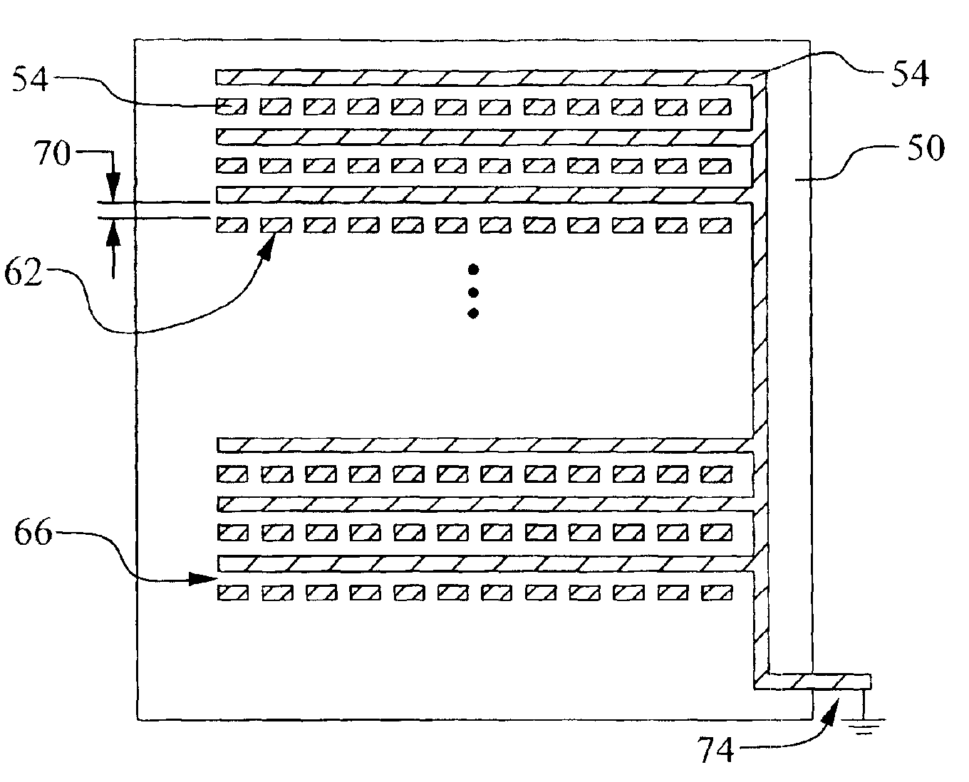
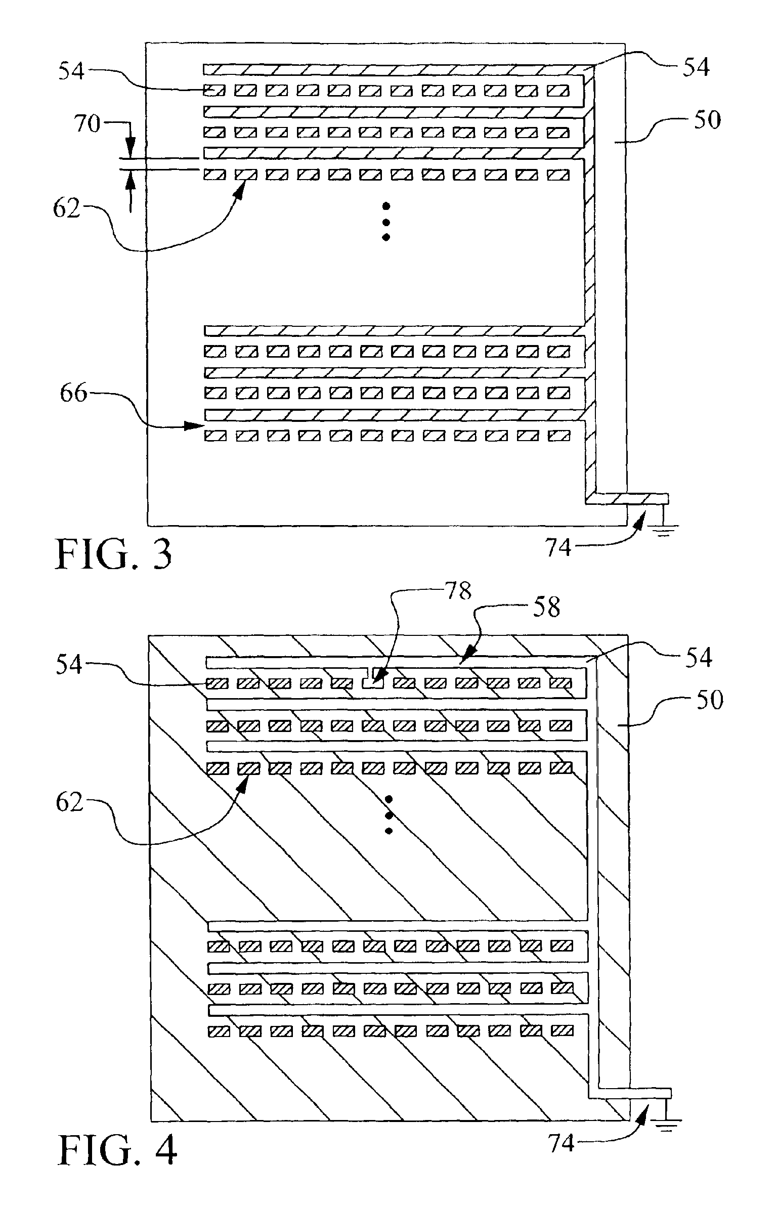
[0032]Referring now to FIGS. 3 and 4, a first preferred embodiment of the present invention is illustrated. A novel test structure for locating bridging defects is disclosed. Several important fea...


PUM


Abstract

A new test structure to locate bridging defects in a conductive layer of an integrated circuit device is achieved. The test structure comprises a line comprising a conductive layer overlying a substrate. The line is coupled to ground. A plurality of rectangles comprises the conductive layer. The rectangles are not connected to the line or to other rectangles. Near edges of the rectangles and of the line are parallel. The rectangles are floating. The test structure is used with a passive voltage contrast test in a scanning electron microscope. A test structure and method to measure critical dimensions is disclosed.

Description

BACKGROUND OF THE INVENTION[0001](1) Field of the Invention[0002]The invention relates to a test structure and method to locate bridging defects in an integrated circuit device, and, more particularly, to a test structure and method to locate bridging defects and to monitor critical dimensions using passive voltage contrast without probing.[0003](2) Description of the Prior Art[0004]Integrated circuit device manufacture requires the formation of material films on the surface of a wafer substrate. These material films are deposited and then patterned. Typical patterning techniques employ a photolithographic step (photo) and an etching step (etch) as is well known in the art. For example, in the formation of the metal interconnect level, a metal material such as aluminum is deposited over the substrate. A photo step is then used to form a patterned photoresist mask overlying the metal. An etch step is then performed where the metal is exposed to an etching atmosphere. The metal layer ...

Claims


Application Information

Patent Timeline
IPC IPC(8): G01R31/311G01R31/28H01L23/544
CPCG01R31/311H01L22/34Y10S257/919Y10S257/911
Inventor SONG, ZHIGANGREDKAR, SHAILESHOH, CHONG KHIAM
Owner CHARTERED SEMICONDUCTOR MANUFACTURING
Why Eureka
Try Eureka