Semiconductor device with nanoclusters

a technology of nanocrystals and semiconductors, applied in the direction of semiconductor devices, electrical equipment, nanotechnology, etc., can solve the problems of oxidizing nanocrystals and undesired increase of the bottom dielectric thickness

Inactive Publication Date: 2005-10-25
TAIWAN SEMICON MFG CO LTD
View PDF3 Cites 50 Cited by
  • Summary
  • Abstract
  • Description
  • Claims
  • Application Information

AI Technical Summary

Problems solved by technology

This steam oxidation process may penetrate the control dielectric of the charge storage transistors thereby undesirably oxidizing the nanocrystals and undesirably increasing the bottom dielectric thickness.

Method used


Image

  • Semiconductor device with nanoclusters
  • Semiconductor device with nanoclusters
  • Semiconductor device with nanoclusters

Examples


first embodiment

[0029]FIGS. 1-6 show partial side views of a semiconductor wafer during stages in the manufacture of a memory including nanoclusters according to the present invention. As will be described later, the method includes utilizing an oxidation barrier layer for inhibiting the oxidation of the nanoclusters and bottom dielectric.

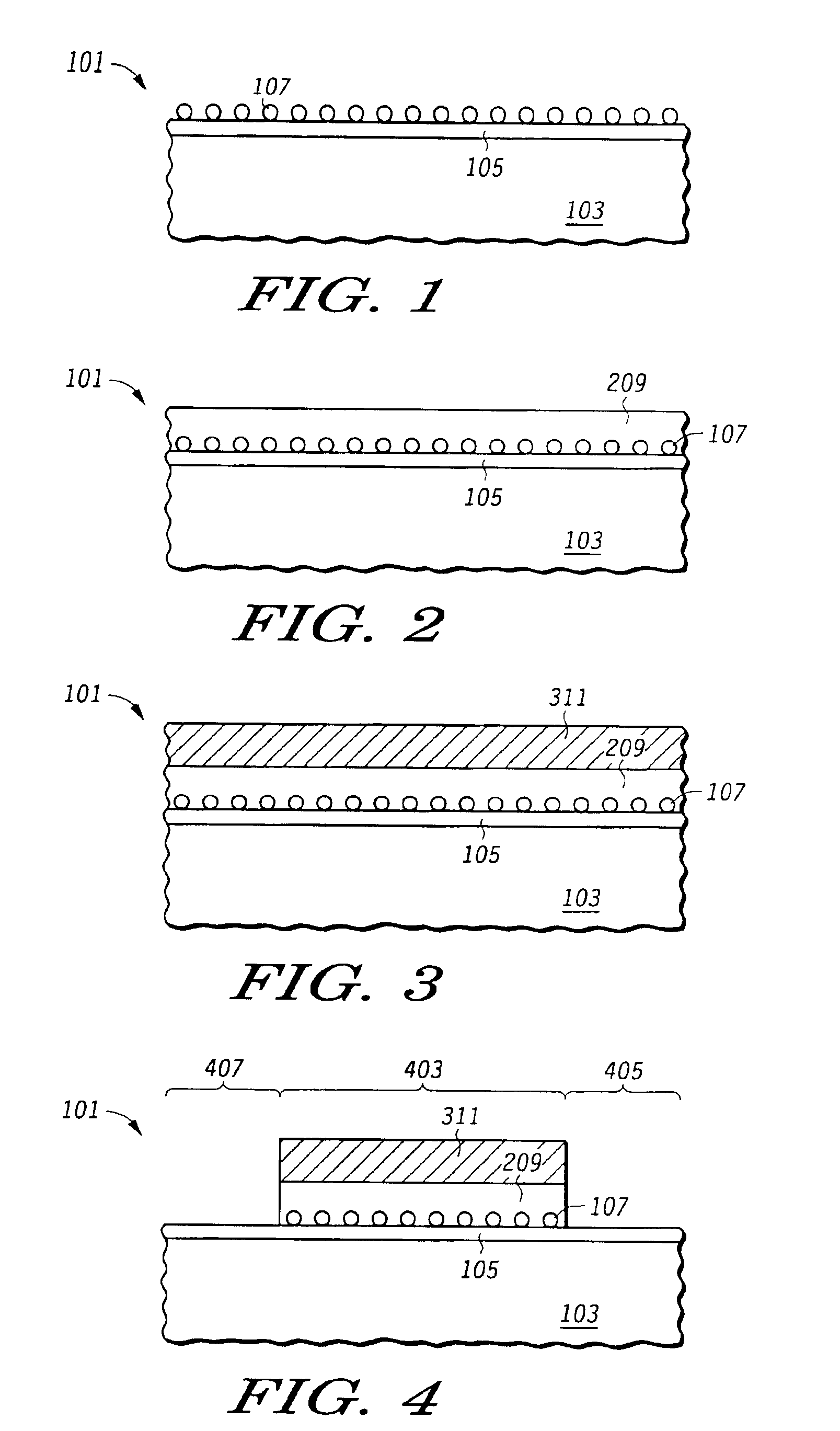
[0030]Referring to FIG. 1, wafer 101 includes a semiconductor substrate 103. A bottom dielectric 105 (e.g. of silicon dioxide, silicon oxynitride, hafnium oxide, aluminum oxide, lanthanum oxide, or lanthanum silicate) has been formed over substrate 103 e.g. by oxidation or chemical vapor deposition. In one embodiment, bottom dielectric has thickness of 5 nanometers, but may be of other thicknesses in other embodiments. A layer of nanoclusters 107 (e.g. of silicon, aluminum, gold, germanium, or a silicon and germanium alloy or other types of conductive material or doped or undoped semiconductive material) is formed over bottom dielectric 105 by e.g. chemical vapor ...

second embodiment

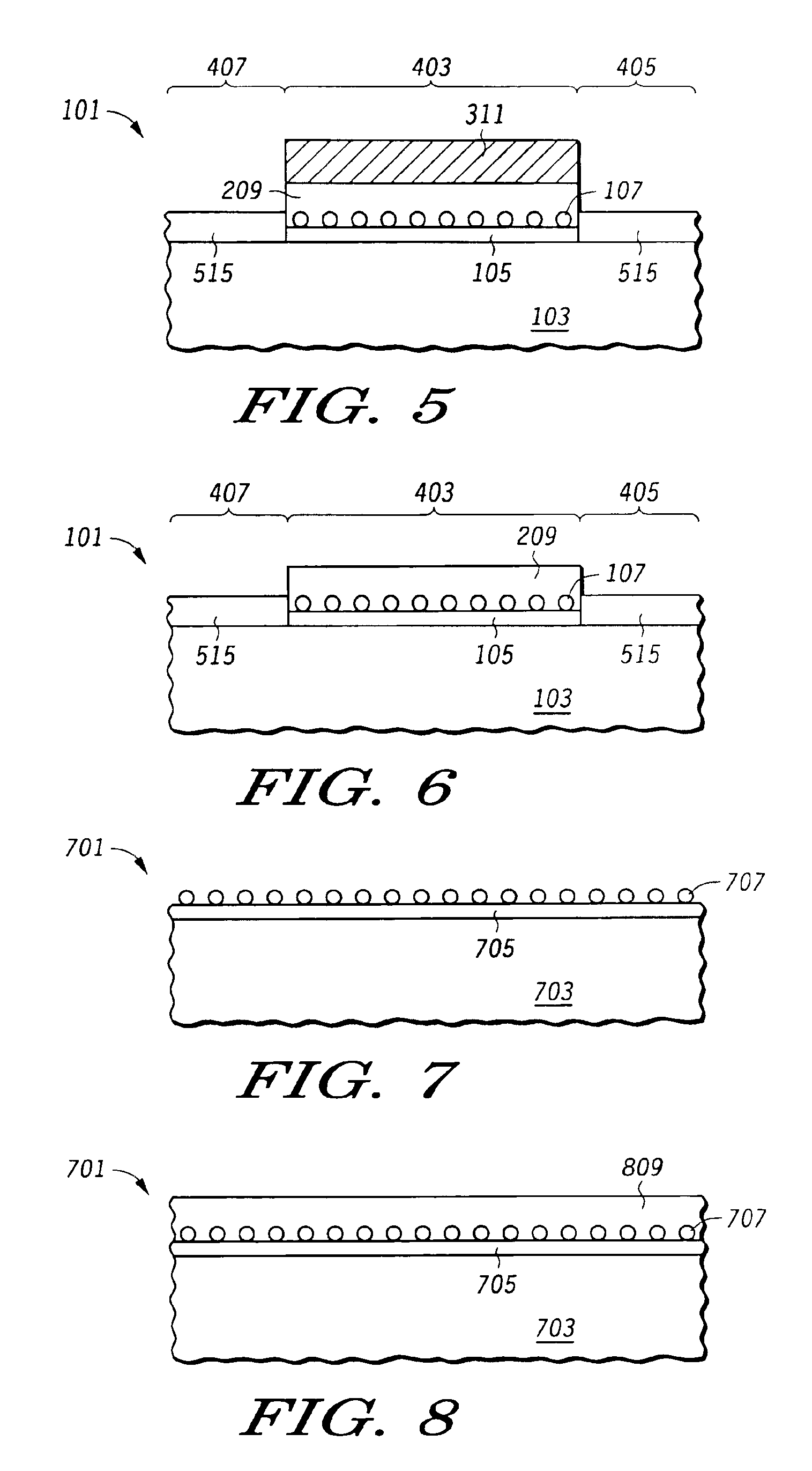
[0041]FIGS. 7-11 show partial side views of a semiconductor wafer during stages in the manufacture of a memory including nanoclusters according to the present invention. Referring to FIG. 7, a bottom dielectric 705 is formed over a substrate 703 of wafer 701. Nanoclusters 707 are then formed over wafer 701.

[0042]Referring to FIG. 8, an oxidation barrier layer 809 is deposited over wafer 701 on nanoclusters 707. The oxidation barrier layer 809 is of a different material than of nanoclusters 707. In one embodiment layer 809 includes silicon nitride, but in other embodiments, layer 809 may include other materials e.g. such as those described above with respect to layer 311.

[0043]Referring to FIG. 9, layer 809, nanoclusters 707, and bottom dielectric 705 are patterned to leave those structures in the memory array areas (e.g. 903) and to remove those structures from other areas (e.g. high voltage area 905).

[0044]Referring to FIG. 10, a dielectric layer 1015 is grown in areas 905 and 907 ...

third embodiment

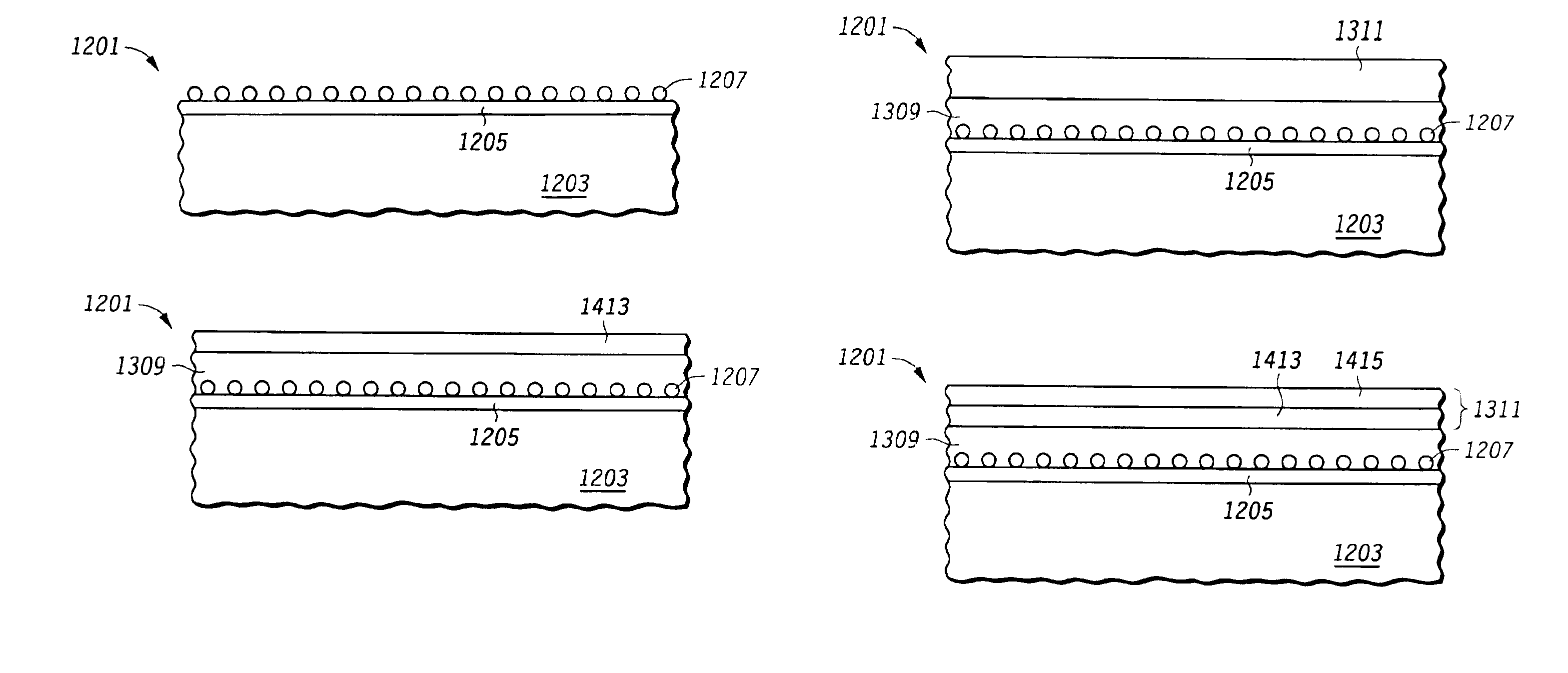
[0047]FIGS. 12-18 show partial side views of a semiconductor wafer during stages in the manufacture of a memory including nanoclusters according to the present invention. Referring to FIG. 12, a bottom dielectric 1205 is formed over a substrate 1203 of wafer 1201. Nanoclusters 1207 are then formed over wafer 101.

[0048]Referring to FIG. 13, a layer of dielectric material (e.g. silicon dioxide) is formed over wafer 1201 by e.g. chemical vapor deposition to form control dielectric 1309. In one embodiment, control dielectric 1309 has a thickness of 5-10 nanometers, but may have other thickness in other embodiments. An oxidation barrier layer 1311 is then deposited over wafer 1201 on dielectric 1309. In one embodiment, layer 1311 includes silicon nitride, but in other embodiments, layer 1311 may include other materials e.g. as those described above with respect to layer 311.

[0049]Referring to FIG. 14, the top portion of barrier layer 1311 is oxidized to form oxidized portion 1415 leaving...


PUM


Abstract

A process of forming a device with nanoclusters. The process includes forming nanoclusters (e.g. silicon nanocrystals) and forming an oxidation barrier layer over the nanoclusters to inhibit oxidizing agents from oxidizing the nanoclusters during a subsequent formation of a dielectric of the device. At least a portion of the oxidation barrier layer is removed after the formation of the dielectric. In one example, the device is a memory wherein the nanoclusters are utilized as charge storage locations for charge storage transistors of the memory. In this example, the oxidation barrier layer protects the nanoclusters from oxidizing agents due to the formation of gate dielectric for high voltage transistors of the memory.

Description

BACKGROUND OF THE INVENTION[0001]1. Field of the Invention[0002]This invention relates to devices with nanoclusters.[0003]2. Description of the Related Art[0004]Some devices such as memories (e.g. non volatile memories) utilize discrete charge storage elements called nanoclusters (e.g. of silicon, aluminum, gold, or germanium) for storing charge in a charge storage location of a transistor. In some examples, the nanoclusters are located between two dielectric layers, a bottom dielectric and a control dielectric. Examples of such transistors include thin film storage transistors. A memory typically includes an array of such transistors. Examples of nanocluster types includes silicon nanocrystals, germanium nanocrystals, gold nanoclusters, and aluminum nanoclusters. In some examples, nanoclusters are from 10-100 Angstroms in sized and may be of doped or undoped semiconductor material or made of conductive materials.[0005]Some memories that have charge storage transistors with nanoclus...

Claims


Application Information

Patent Timeline
Patent Type & Authority Patents(United States)
IPC IPC(8): H01L21/336H01L21/70H01L21/02H01L21/8238H01L21/28H01L27/115H01L29/423
CPCB82Y10/00H01L21/28273H01L27/115H01L29/42332H01L29/40114H10B69/00H01L27/105B82Y40/00
Inventor STEIMLE, ROBERT F.MURALIDHAR, RAMACHANDRANPAULSON, WAYNE M.RAO, RAJESH A.WHITE, JR., BRUCE E.PRINZ, ERWIN J.
Owner TAIWAN SEMICON MFG CO LTD
Why Eureka
Try Eureka