Thermally operated switch control memory cell

a switch control and memory cell technology, applied in the direction of transistors, solid-state devices, instruments, etc., can solve the problems of cell more subject to magnetic state, difficult production of high-yield cells, and complex magnetic environmen

Active Publication Date: 2005-11-08
NVE CORP
View PDF14 Cites 65 Cited by
  • Summary
  • Abstract
  • Description
  • Claims
  • Application Information

AI Technical Summary

Benefits of technology

[0031]The present invention provides a ferromagnetic thin-film based digital memory having a substrate supporting bit structures separated from one another by spacer material that are electrically interconnected with information storage and retrieval circuitry and having magnetic material films in which a characteristic magnetic property is substantially maintained below an associated critical temperature above which such magnetic property is not maintained of which two are separated by at least one layer of a nonmagnetic material having two major surfaces on opposite sides thereof with these bit structures each having an interconnection structure providing electrical contact thereto positioned against a contact surface thereof substantially parallel to the intermediate layer major surfaces and also being between the contact surface and the substrate. There is also a plurality of word line structures each located across from a corresponding one of the bit structures on an opposite side of the intermediate layer of a corresponding one of said bit structures from the first interconnection structure providing electrical contact thereto. The information storage and retrieval circuitry can draw a sufficient electrical current selectively through each of these bit structures and its interconnection structure providing electrical contact thereto to cause substantial heating of that bit structure to raise temperatures thereof to have at least one of the magnetic material films therein at least approach its corresponding associated critical temperature while being substantially above temperatures of at least an adjacent said bit structure because of sufficient extent of, and smallness of thermal conductivities of, at least portions of the selected bit structure and of those portions of the substrate and the spacer material positioned thereabout.

Problems solved by technology

In this situation, the magnetic environment can become quite complex with fields in any one memory cell affecting the film portions in neighboring memory cells.
Also, small ferromagnetic film portions in a memory cell can lead to substantial demagnetization fields which can cause instabilities in the magnetization state desired in such a cell.
One of the difficulties in such memories is the need to provide memory cells therein that have extremely uniform switching thresholds and adequate resistance to unavoidable interjected magnetic field disturbances in the typical memory cell state selection scheme used.
Such a coincident interjected magnetic fields memory cell state selection scheme is very desirable in that an individual switch, such as that provided by a transistor, is not needed for every memory cell, but the limitations this selection mode imposes on the uniformity of switching thresholds for each memory cell in a memory make the production of high yields difficult.
As such magnetic thin-film memory cells are made smaller to thereby increase the cell density over the surface of the substrate on which they are disposed, the resulting cells become more subject to magnetic state, or data, upsets due to thermal fluctuations occurring in the materials therein.
However, the trade-off between thermal stability and magnetic stability is a serious problem when the total magnetic volume of bits is less than about 104 to 105 nm3.
Although the required barrier energy to be thermally stable can be reduced by use of error correction and periodic retrievals with corresponding corrections of the data stored in the whole memory, such a memory takes additional chip area and increased processing steps thereby increasing costs and reducing operating rapidity.
However, the magnetization direction in this composite layer by itself is not very strongly fixed in any direction because of the relatively weak anisotropy exhibited by the ferromagnetic layers.
Generating such magnetic fields begins to require currents through such cells and associated word lines of magnitudes that result in current densities sufficient to cause significant electromigration of the conductive materials and operating temperature rises of the cell region which will alter device behavior and structure.
Such effects thereby lead to a limit of some minimum size for these cells.
Such magnetic selection schemes for data retrievals introduce further data disturbance opportunities through again generating magnetic fields that can combine with unwanted magnetic fields that appear.
However, this arrangement dissipates heat along the entire sense line and along the entire word line carrying these currents to thereby result in substantial power dissipation and heating of otherwise unselected cells.

Method used


Image

  • Thermally operated switch control memory cell
  • Thermally operated switch control memory cell
  • Thermally operated switch control memory cell

Examples


Embodiment Construction

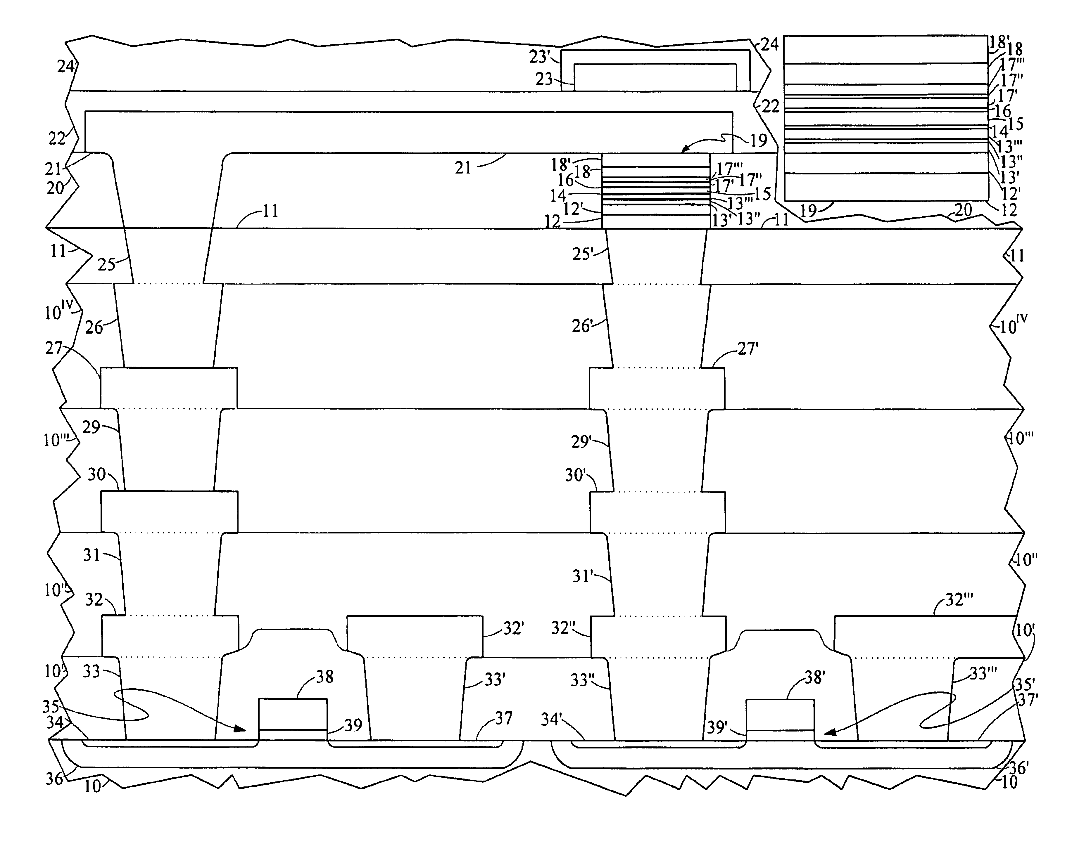
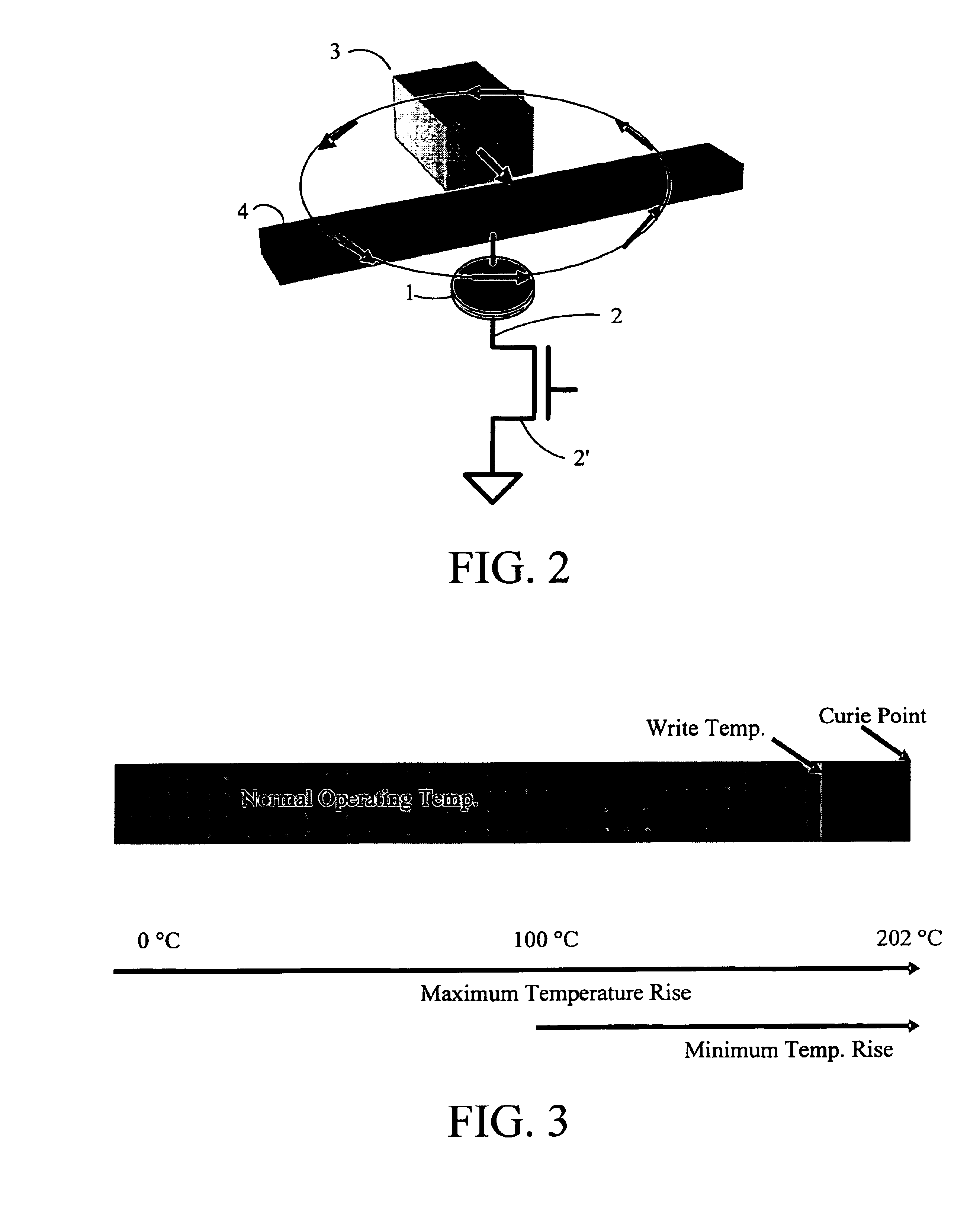
[0042]FIG. 2 shows a schematic representation of a memory cell arrangement that uses a combination of heat and magnetic fields to store data in a cell structure, 1. This device is part of a two dimensional area based array of such cells, typically formed on a substrate, 2, containing a monolithic integrated circuit including switching transistors such as a MOSFET, 2′, in which a selected cell 1 is at the intersection of (a) one of many word line conductors, 3, in being adjacent thereto, which conductor provides magnetic fields by the current supplied therethrough but little heat, and of (b) a current supply line, 4, connected to cell structure 1 that structure further, in turn, being connected the corresponding cell selection switching transistor 2′ having a source or drain thereof connected to cell structure 1. Transistor 2′ is switched into an “on” condition by applying suitable electrical potentials to supply line 4 and to the gate thereof with the remaining one of the transistor...


PUM


Abstract

A ferromagnetic thin-film based digital memory having a substrate supporting bit structures that are electrically interconnected with information storage and retrieval circuitry and having magnetic material films in which a characteristic magnetic property is substantially maintained below an associated critical temperature above which such magnetic property is not maintained separated by at least one layer of a nonmagnetic material with each bit structure having an interconnection structure providing electrical contact thereto at a contact surface thereof substantially parallel to the intermediate layer positioned between the first contact surface and the substrate. A plurality of word line structures located across from a corresponding one of the bit structures on an opposite side of the intermediate layer of a corresponding one of said bit structures from its interconnection structure provides electrical contact thereto. Sufficient electrical current selectively drawn through each of these bit structures and its interconnection structure can cause substantial heating of that bit structure to raise temperatures thereof to have at least one of the magnetic material films therein at least approach its corresponding associated critical temperature while being substantially above temperatures of at least an adjacent said bit structure because of sufficient thermal isolation.

Description

CROSS-REFERENCE TO RELATED APPLICATION(S)[0001]This application claims the benefit of Provisional Application No. 60 / 483,371 filed on Jun. 23, 2003 for “THERMALLY OPERATED SWITCH CONTROL MEMORY CELL”.BACKGROUND OF THE INVENTION[0002]The present invention relates to ferromagnetic thin-film structures exhibiting relatively large magnetoresistive characteristics and, more particularly, to such structures used for the storage and retrieval of digital data.[0003]Many kinds of electronic systems make use of magnetic devices including both digital systems, such as memories, and analog systems such as magnetic field sensors. Digital data memories are used extensively in digital systems of many kinds including computers and computer systems components, and digital signal processing systems. Such memories can be advantageously based on the storage of digital symbols as alternative states of magnetization in magnetic materials provided in each memory storage cell, the result being memories whi...

Claims


Application Information

Patent Timeline
Patent Type & Authority Patents(United States)
IPC IPC(8): G11C11/00H01L31/115H01L31/119G01RG11C11/16
CPCG11C11/16H01L27/228H01L43/10H10B61/22H10N50/85
Inventor DAUGHTON, JAMES M.POHM, ARTHUR V.
Owner NVE CORP
Why Eureka
Try Eureka