

Wafer level microelectronic packaging with double isolation
a technology of microelectronic elements and packaging, applied in the field of microwave-level microelectronic packaging, can solve the problems of adding cost and bulk to the assembly, adding to the cost of the overall system, and adding to the cost of the system, and achieve excellent thermal isolation of the microelectronic elemen
- Summary
- Abstract
- Description
- Claims
- Application Information
AI Technical Summary
Benefits of technology
Problems solved by technology
Method used
Image

Examples
Embodiment Construction
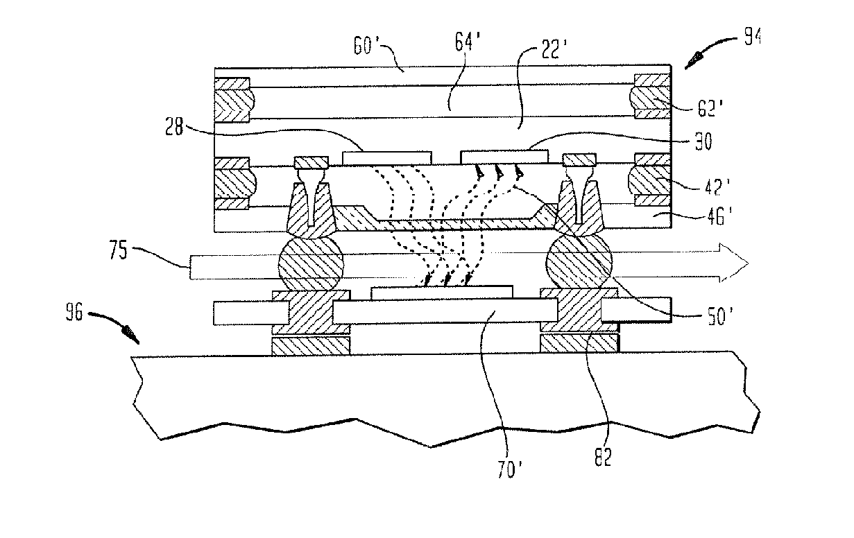
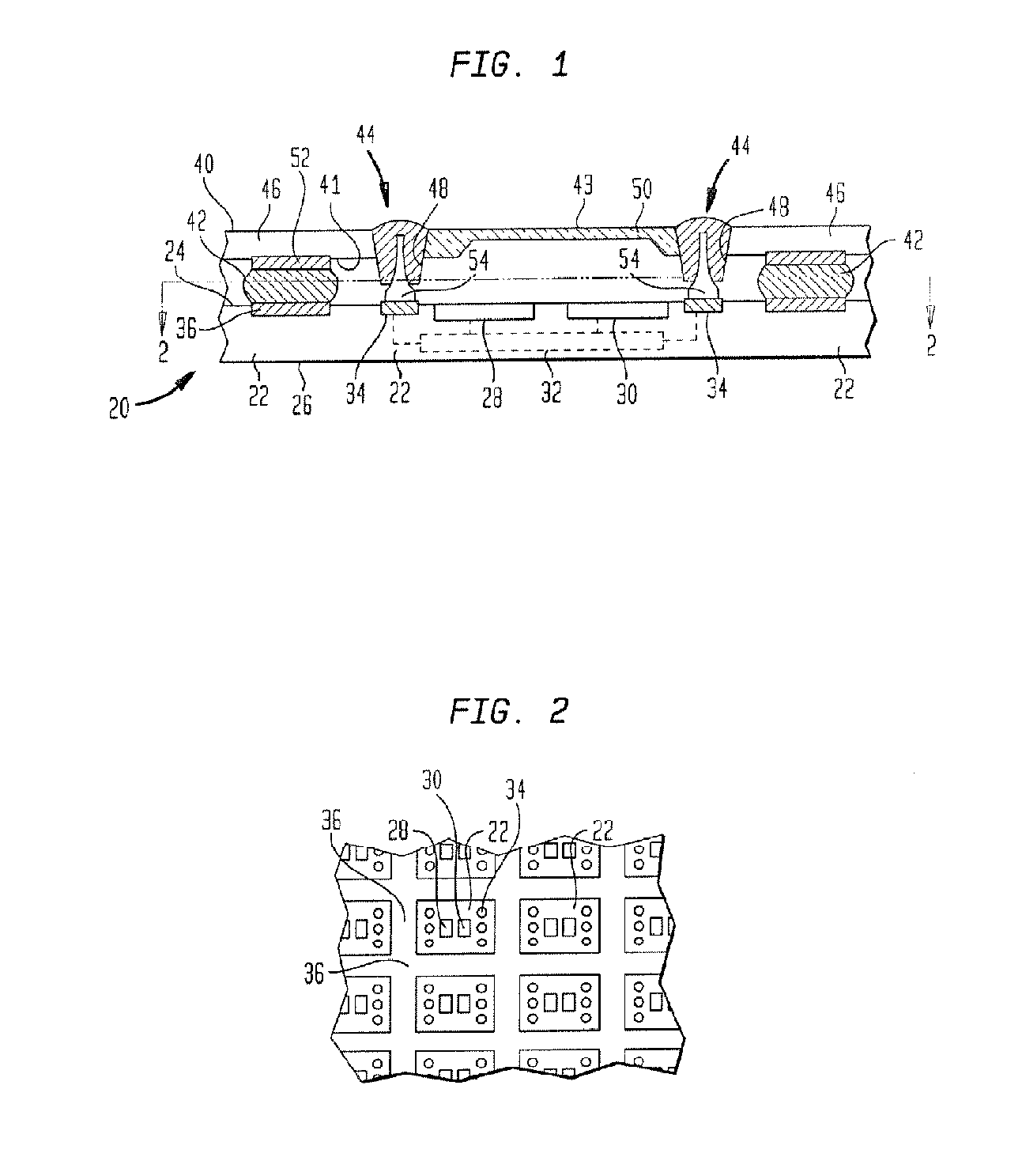
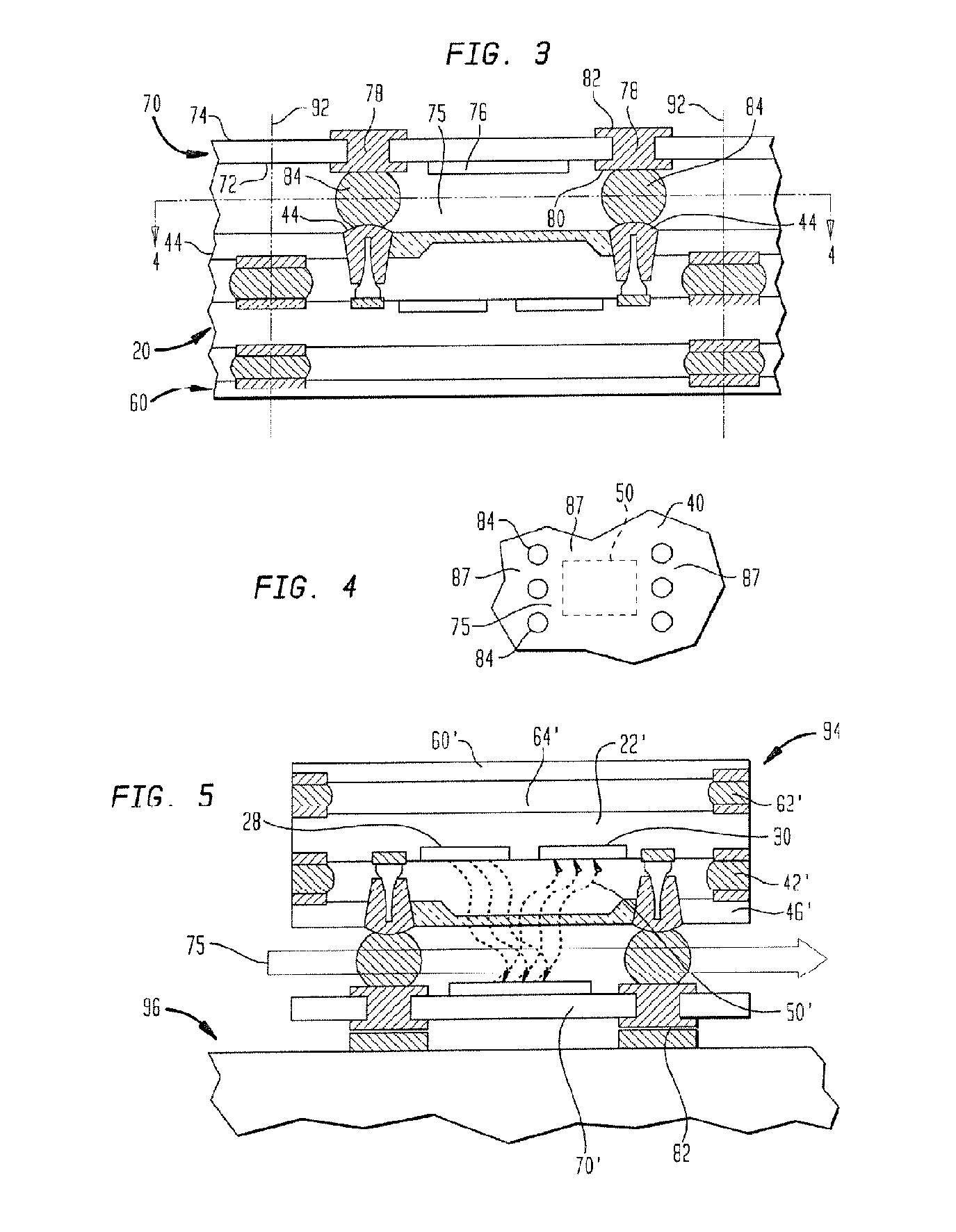
[0025] A fabrication process according to one embodiment of the present invention utilizes a wafer 20, referred to herein as the “main wafer.” Wafer 20 includes a plurality of individual regions 22 formed as an integral unit. Wafer 20 typically is formed as a unitary body of semiconductor material such as silicon or a compound semiconductor as, for example, silicon carbide or a III-V compound semiconductor such as gallium arsenide, indium gallium arsenide or the like. The wafer may include plural semiconductors as, for example, features formed from one or more compound semiconductors on an underlying layer of silicon or silicon carbide material, together with additional material such as insulators and metallic conductors. The wafer has a front surface 24 and a rear surface 26. Each region 22 includes an emitter 28 adapted to emit radiant energy in a preselected wavelength band. For example, the emitter may incorporate one or more light-emitting diodes or lasers. The emitter is adapt...
PUM
 Abstract
Description
Claims
Application Information