Methods for integrated circuit module packaging and integrated circuit module packages

a technology of integrated circuit modules and packaging methods, applied in the direction of electrical equipment, semiconductor devices, semiconductor/solid-state device details, etc., can solve the problems of reducing performance, affecting the performance of the device, and unable to achieve higher integration levels

Active Publication Date: 2008-11-04
SKYWORKS SOLUTIONS INC
View PDF10 Cites 85 Cited by
  • Summary
  • Abstract
  • Description
  • Claims
  • Application Information

AI Technical Summary

Problems solved by technology

In high frequency applications achieving higher levels of integration is hindered by increased interference brought on by devices being in closer proximity.
For example, obtaining higher levels of integration can be difficult with radios containing components that are electromagnetically sensitive to interference, such as voltage controlled oscillators (VCO), and power amplification chains that produce electromagnetic radiation that may interfere with VCO functions.
In high frequency applications, another hindrance to integration is thermal coupling between a heat source such as a power amplifier and thermally sensitive components such as Surface Acoustical Wave (SAW) filters and duplexers, whose performance may be degraded by elevated temperatures generated by the power amplifier.
Furthermore, heat generated within the power amplifier can cause problems within the power amplifier itself and require additional circuit complexity to deal with thermal runaway, bias compensation, or calibration compensation.
The “cans” also add undesirable size and cost to the final application and may cause electromagnetic coupling feedback loops.

Method used


Image

  • Methods for integrated circuit module packaging and integrated circuit module packages
  • Methods for integrated circuit module packaging and integrated circuit module packages

Examples


Embodiment Construction

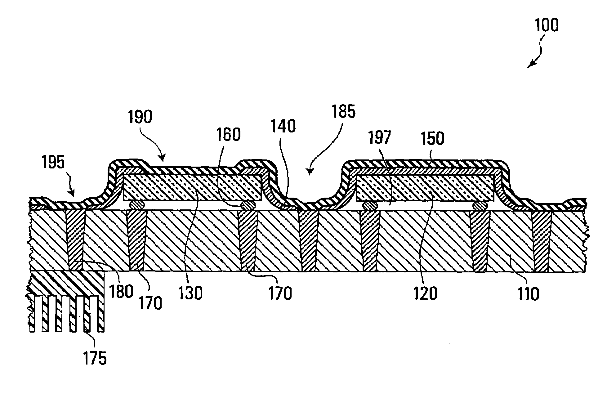
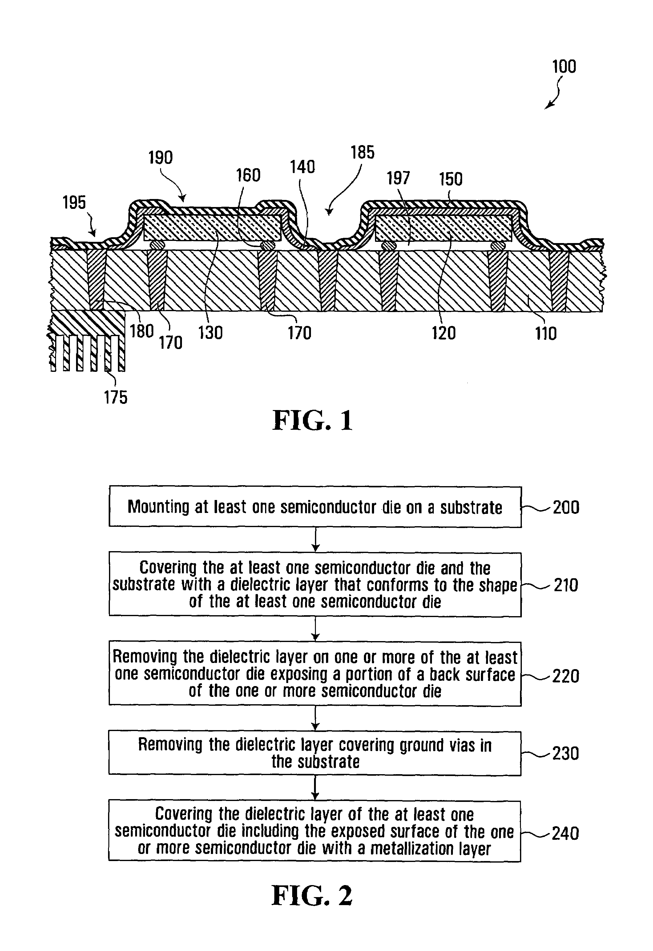
[0013]FIG. 1 shows a cross section of a portion of an integrated circuit (IC) module package, generally indicated at 100, according to an embodiment of the invention. The package includes a common module substrate 110, a first semiconductor die 120, a second semiconductor die 130, each of the semiconductor dies 120,130 mounted to the common module substrate 110 and each semiconductor die including an IC component (not shown). The package includes solder bumps 160 for attaching the first and second semiconductor dies 120,130 to the common module substrate 110. The solder bumps 160 also electrically connect the respective dies to substrate metal tracks or vias. A dielectric layer 140 is shown to cover the common module substrate 110, the first semiconductor die 120 and partially cover the second semiconductor die 130, with the exception of an opening 190 in the dielectric layer 140 on a top surface of the second semiconductor die 130. The application of the dielectric layer 140 create...


PUM


Abstract

In order to achieve electromagnetic and / or thermal isolation between components in close proximity to each other on a common module substrate, an alternate package and method for manufacturing the package is provided.Inventive methods utilize a grounded, metal-coated overmold for a IC module package that can provide an alternate thermal path to heat sink high power components generating excess heat energy and / or provide general electromagnetic shielding and isolation between two integrated circuits in very close proximity that are susceptible to electromagnetic interference.A dielectric layer conformably covers semiconductor dies mounted on a substrate. On some semiconductor dies, a portion of the dielectric layer is removed from the back surface of the semiconductor dies to allow direct contact between the exposed back surface of the dies and a metallization layer forming part of the overmold. This direct contact allows heat energy to be drawn away from the dies. The metallization layer also acts to shield the dies from disruptive electromagnetic energy radiated from other dies in close proximity.

Description

FIELD OF THE INVENTION[0001]The invention relates to integrated circuit (IC) packaging methods, in particular methods for manufacturing packages having thermal isolation and electromagnetic shielding.BACKGROUND OF THE INVENTION[0002]In IC manufacturing, in particular manufacturing semiconductor components used in devices such as wireless radios, there is a desire to combine higher levels of functionality with a higher level of integration. In high frequency applications achieving higher levels of integration is hindered by increased interference brought on by devices being in closer proximity. For example, obtaining higher levels of integration can be difficult with radios containing components that are electromagnetically sensitive to interference, such as voltage controlled oscillators (VCO), and power amplification chains that produce electromagnetic radiation that may interfere with VCO functions. It is desirable to provide electromagnetic isolation between the two components so...

Claims


Application Information

Patent Timeline
Patent Type & Authority Patents(United States)
IPC IPC(8): H01L21/44H01L21/48
CPCH01L23/3677H01L23/552H01L25/0655H03H9/1078H01L23/66H01L2224/16235H01L2924/01078H01L2924/01079H01L2924/3025H01L2224/16H03H9/02834
Inventor HARRISON, JOSENUNNS, NICHOLASVAILLANCOURT, WILLIAM
Owner SKYWORKS SOLUTIONS INC
Why Eureka
Try Eureka