Critical dimension analysis with simultaneous multiple angle of incidence measurements

a technology of incidence measurement and critical dimension analysis, applied in the field of optical metrology equipment, can solve the problems of inability to clearly distinguish features, inability to perform rigorous analysis, and inability to achieve the effect of maximizing the information content of measurement and increasing the ability to unambiguously distinguish features

Inactive Publication Date: 2005-12-06
THERMA WAVE INC
View PDF19 Cites 184 Cited by
  • Summary
  • Abstract
  • Description
  • Claims
  • Application Information

AI Technical Summary

Benefits of technology

[0012]It is believed that the data generated by either of these tools could be used to appropriately model and analyze critical dimensions and feature profiles on semiconductors.
[0017]Alternatively or in addition, the measurement data which can be obtained from two or more metrology devices of the type described in the above identified PCT application, could be used to advance this analysis. As more of these metrology devices are added, the ability to unambiguously distinguish features increases. Thus, it is within the scope of the subject invention to utilize either or both of a simultaneous multiple angle of incidence spectrometer or ellipsometer along with one or more of spectroscopic reflectometry, spectroscopic ellipsometry or absolute ellipsometry tools with the latter two being deployed in a manner that maximizes the information content of the measurement. For example, with a rotating compensator spectroscopic ellipsometer one measures both the sign and magnitude of the ellipsometric phase while in more standard configurations, e.g., a rotating polarizer / rotating analyzer, only the magnitude or phase can be measured.

Problems solved by technology

In the past, this type of rigorous analysis was limited to the research environment, since the calculations necessary to determine the periodic structure was extremely complex and time consuming.

Method used


Image

  • Critical dimension analysis with simultaneous multiple angle of incidence measurements
  • Critical dimension analysis with simultaneous multiple angle of incidence measurements
  • Critical dimension analysis with simultaneous multiple angle of incidence measurements

Examples


Embodiment Construction

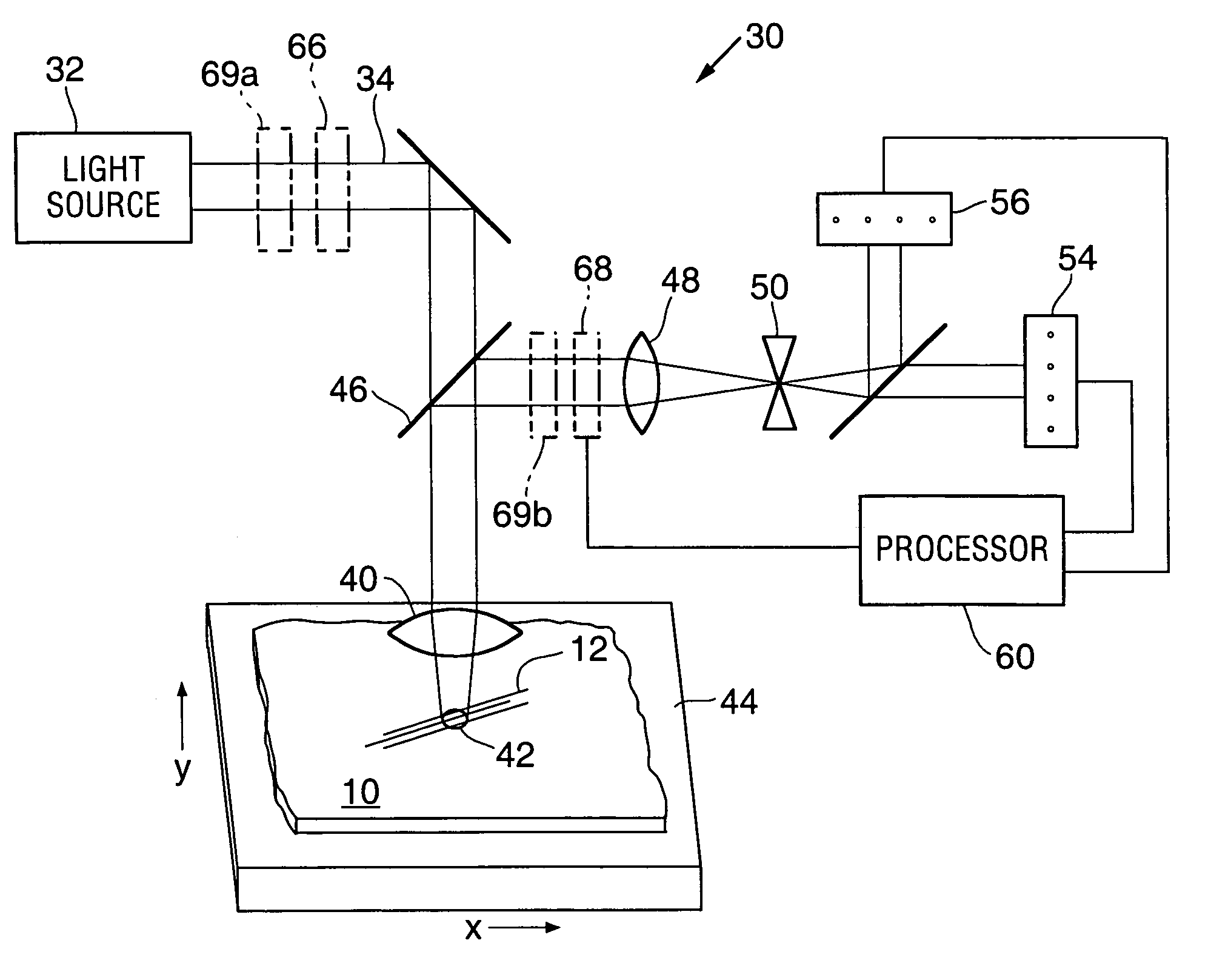
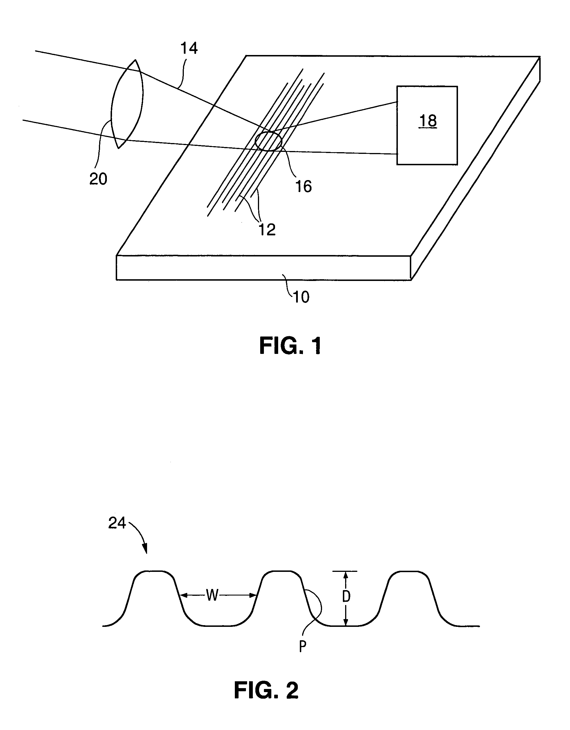
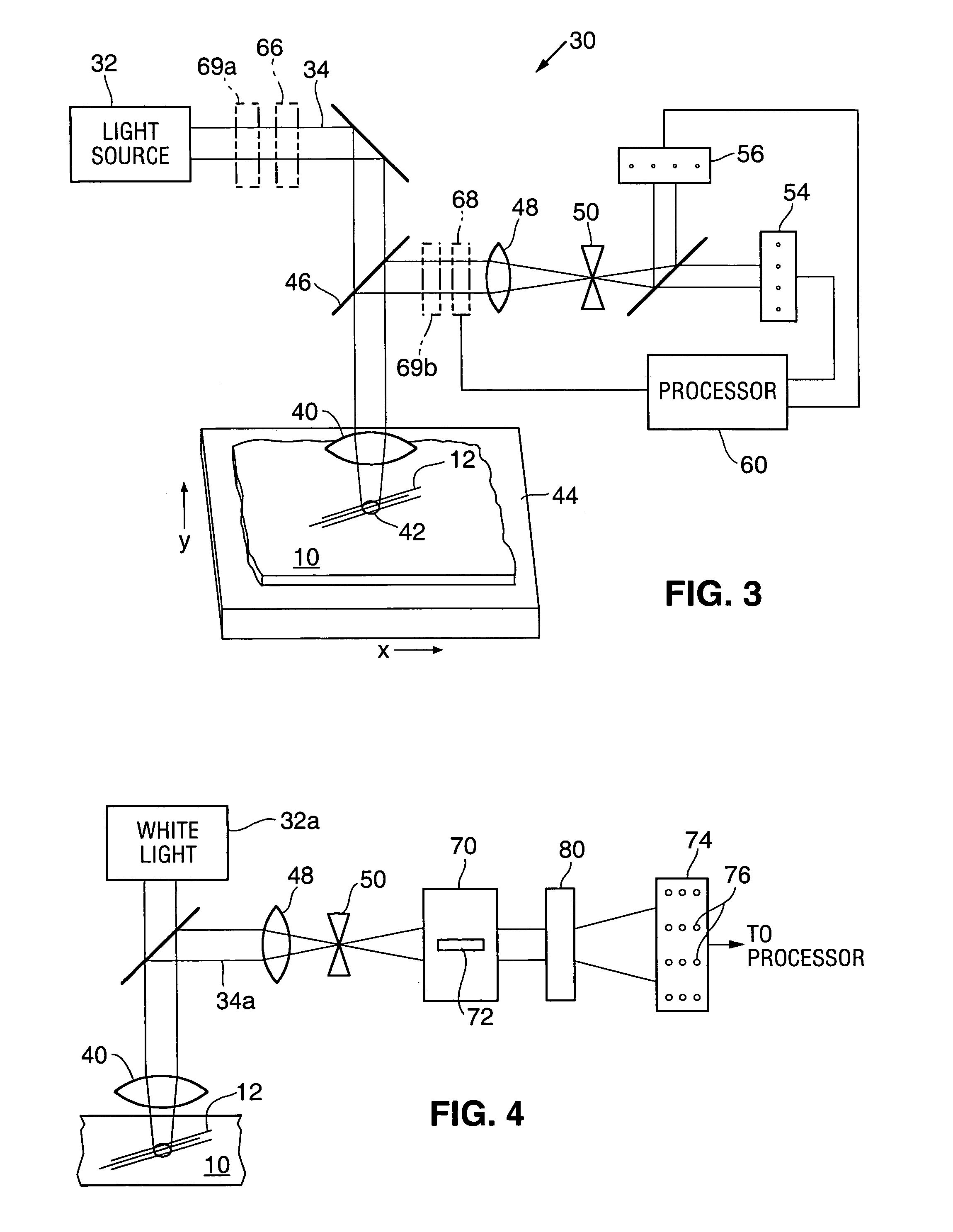
[0024]Turning to FIG. 3, a basic schematic of simultaneous multiple angle of incidence apparatus 30 is illustrated. Further details about such a device are described in U.S. Pat. Nos. 4,999,014; 5,042,951; 5,159,412 and 5,412,473 all incorporated herein by reference. As noted above, the assignee's Opti-Probe device incorporates portions of this technology and markets the measurement subsystem under the trademark Beam Profile Reflectometry or BPR. In the past, the BPR technology was utilized primarily to analyze the characteristics of thin films formed on semiconductors. This disclosure is directed to using the measurements which can be obtained from this type of system to evaluate the geometry of periodic structures formed on semiconductors.

[0025]The basic measurement system includes a light source 32 for generating a probe beam 34. The light source can be a laser for generating a coherent beam of radiation. Laser diodes are suitable laser sources for this application. If the output...


PUM


Abstract

A method and apparatus are disclosed for evaluating relatively small periodic structures formed on semiconductor samples. In this approach, a light source generates a probe beam which is directed to the sample. In one preferred embodiment, an incoherent light source is used. A lens is used to focus the probe beam on the sample in a manner so that rays within the probe beam create a spread of angles of incidence. The size of the probe beam spot on the sample is larger than the spacing between the features of the periodic structure so some of the light is scattered from the structure. A detector is provided for monitoring the reflected and scattered light. The detector includes multiple detector elements arranged so that multiple output signals are generated simultaneously and correspond to multiple angles of incidence. The output signals are supplied to a processor which analyzes the signals according to a scattering model which permits evaluation of the geometry of the periodic structure. In one embodiment, the sample is scanned with respect to the probe beam and output signals are generated as a function of position of the probe beam spot.

Description

PRIORITY[0001]This application is a continuation of U.S. application Ser. No. 10 / 658,176, filed Sep. 9, 2003 now U.S. Pat. No. 6,829,057, which is in turn a continuation of U.S. application Ser. No. 10 / 150,032, filed May 17, 2002, now U.S. Pat. No. 6,654,131, which is in turn a continuation of U.S. application Ser. No. 09 / 818,703, filed Mar. 27, 2001, now U.S. Pat. No. 6,429,943, which claimed priority to provisional application Ser. No. 60 / 192,899, filed Mar. 29, 2000, incorporated herein by reference.TECHNICAL FIELD[0002]The subject invention relates to optical metrology equipment for measuring critical dimensions and feature profiles of periodic structures on semiconductor wafers. The invention is implemented using data obtained from simultaneous multiple angle of incidence measurements as an input to analytical software designed to evaluate surface features via a specular scatterometry approach.BACKGROUND OF THE INVENTION[0003]There is considerable interest in the semiconductor ...

Claims


Application Information

Patent Timeline
Patent Type & Authority Patents(United States)
IPC IPC(8): G01B11/02G01B11/14
CPCG01B11/02G01B11/024G01B11/14G03F7/70625
Inventor OPSAL, JONROSENCWAIG, ALLAN
Owner THERMA WAVE INC
Why Eureka
Try Eureka