Method for determining semiconductor overlay on groundrule devices

a groundrule device and semiconductor technology, applied in semiconductor/solid-state device testing/measurement, semiconductor/solid-state device details, instruments, etc., can solve problems such as errors in the measured structure overlay to the printed circuit overlay, and the error prediction of the kerf to the device overlay is an industry wide issue, so as to achieve easy discernability

Inactive Publication Date: 2005-12-13
GLOBALFOUNDRIES INC
View PDF39 Cites 20 Cited by
  • Summary
  • Abstract
  • Description
  • Claims
  • Application Information

AI Technical Summary

Benefits of technology

[0013]In the method and wafer of the present invention, preferably the first and second active circuit features corresponding to the first and second layer kerf measurement features are in contact with each other. The first and second layers of the integrated circuit each may have a plurality of circuit areas separated by kerf areas. Preferably, the second layer kerf measurement feature is displaced from the first layer kerf measurement feature by a distance sufficient to distinguish the corresponding active features in the circuit area so that the first and second layer kerf measurement features are more easily discerned. The common points of reference of the first and second layer kerf measurement features may comprise centerlines or edges of the features. The measurement features in the kerf areas are adapted to be destroyed when the plurality of circuit areas are cut apart.

Problems solved by technology

Kerf to device overlay error prediction is an industry wide issue.
A problem of conventional overlay metrology technique is that the printed structure used in the measurement is printed at a much larger size and different shape than that of the printed circuit.
Due to the physics of optical lithography, mask making and the like, this can lead to errors in the measured structure overlay to that of the printed circuit overlay.
In addition, typical high resolution methods of measuring in-chip overlay such as scanning electron microscopy (SEM) are complicated by the required direct placement of subsequent patterns on top of each other.
This leads to difficulty or even impossibility of measuring the overlay directly in the product chip device since the structures typically sit on top of each other and it may be difficult to discern an edge of a device feature on one level from an edge of a device feature on another level. At sub 0.3 μm ground rules, the magnitude of the problem starts to become a potentially significant contribution to yield loss due to overlay error.

Method used


Image

  • Method for determining semiconductor overlay on groundrule devices
  • Method for determining semiconductor overlay on groundrule devices
  • Method for determining semiconductor overlay on groundrule devices

Examples


Embodiment Construction

)

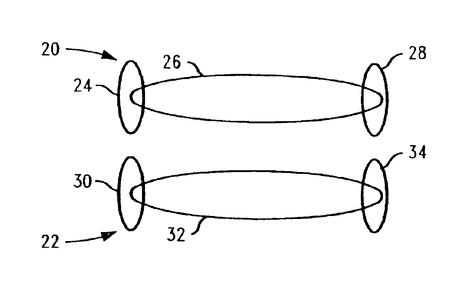
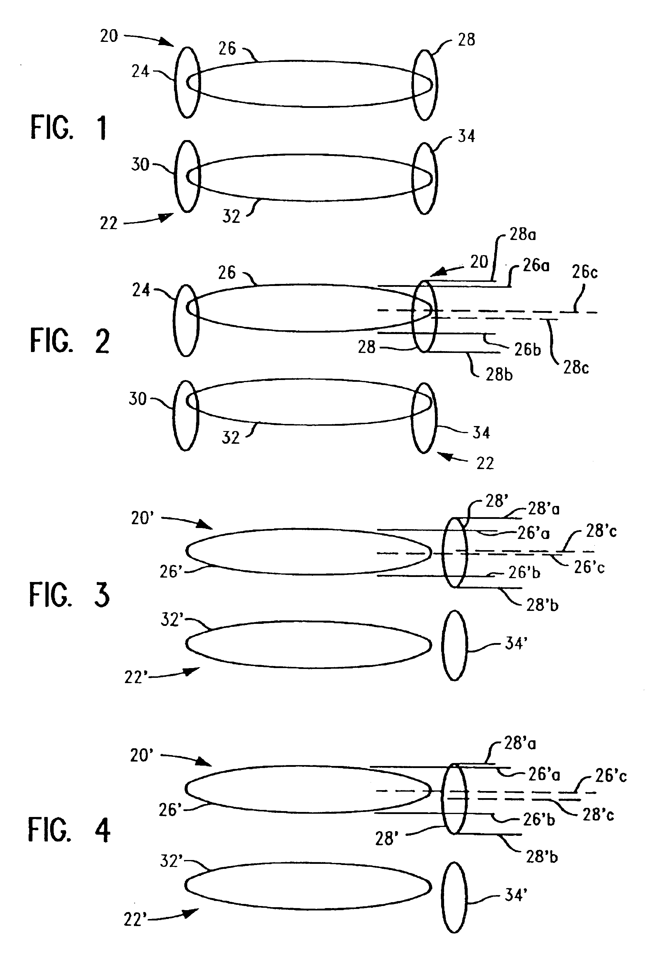
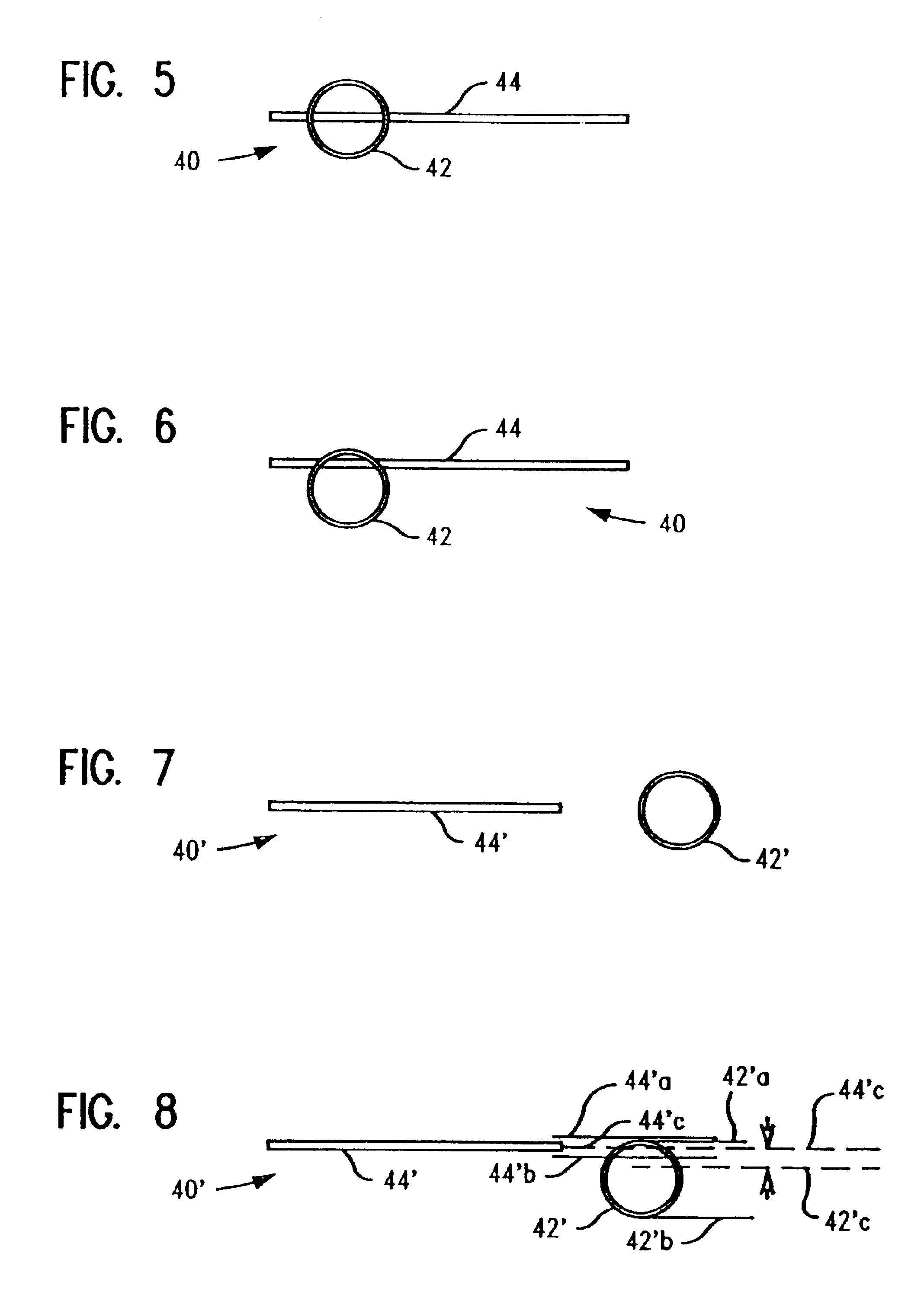
[0029]In describing the preferred embodiment of the present invention, reference will be made herein to FIGS. 1-14 of the drawings in which like-numerals refer to like features of the invention. Features of the invention are not necessarily shown to scale in the drawings.

[0030]In order to easily correlate the conventional overlay measurement to device overlay, the present invention provides a system and method of representing a measurable device structure in the kerf area, between the printed functional circuit areas, to aid in direct device overlay measurement. The present invention is based on a method that allows the overlay to be determined on circuit size and shaped device patterns without the difficulty related to pattern-on-pattern placement. To accomplish this, in the preferred embodiment the device design itself is printed in the kerf, with two patterns being printed not on top of each other, but physically separated in at least one dimension. This permits the use of high ...


PUM

PropertyMeasurementUnit
sizeaaaaaaaaaa
areasaaaaaaaaaa
distanceaaaaaaaaaa

Abstract

A method of determining overlay error comprises creating a first and second layers of an integrated circuit, each having an active circuit feature and an adjacent kerf area. Each kerf area includes a first measurement feature separated from and corresponding substantially to the layer's active circuit feature. The circuit and kerf areas of the layers are substantially superimposed. The distance of separation between the active circuit feature and the layer kerf measurement feature in each layer in the direction of overlay error is the same. The second layer kerf measurement feature is displaced from the first layer kerf measurement feature in a direction perpendicular to the direction that the overlay error is to be determined. Overlay error is determined by measuring distance of separation in the direction of overlay error between the common points of reference of each of the first and second layer kerf measurement features.

Description

BACKGROUND OF THE INVENTION[0001]1. Field of the Invention[0002]The present invention relates to the manufacture of integrated circuits and, in particular, to a method and system for determining overlay error between circuit layers made by a lithographic process.[0003]2. Description of Related Art[0004]Semiconductor manufacturing involves the printing of multiple integrated circuit patterns using lithographic methods on successive levels of exposure tools. A requirement of semiconductor manufacturing is to keep the alignment of each level to previous levels below product tolerance. Currently this is done using the optical microscope based tool that measures structures printed in the field kerf outside the product cell that comprises the printed circuit pattern. The field kerf is the area which separates the individual cells or patterns and which is unusable due to the width of the blade used to cut apart the cells or patterns upon completion of the printing. These structural feature...

Claims


Application Information

Patent Timeline
Patent Type & Authority Patents(United States)
IPC IPC(8): G03F7/20H01L23/544
CPCG03F7/70633H01L22/34
Inventor AUSSCHNITT, CHRISTOPHER P.MUTH, WILLIAM A.
Owner GLOBALFOUNDRIES INC
Why Eureka
Try Eureka