Multiple testing bars for testing liquid crystal display and method thereof

Inactive Publication Date: 2006-01-03
SAMSUNG DISPLAY CO LTD
View PDF8 Cites 16 Cited by
  • Summary
  • Abstract
  • Description
  • Claims
  • Application Information

AI Technical Summary

Benefits of technology

[0030]In this test method according to the present invention, it is possible to detect short-circuited defects bet

Problems solved by technology

However, if more than two gate lines or data lines, for example, the data lines D2 and D3 in FIG. 1, are short-circuited (S1), it is hard to detect the short-circuited element

Method used


Image

  • Multiple testing bars for testing liquid crystal display and method thereof
  • Multiple testing bars for testing liquid crystal display and method thereof
  • Multiple testing bars for testing liquid crystal display and method thereof

Examples


second embodiment

[0067]A second embodiment shown in FIG. 7 has a structure in which the additional step of removing the gate shorting bar is not required before the array tests.

[0068]The structure of the connection between the first and the second secondary lines 410 and 420 and the gate extensions 101, 102 and 103 in the second embodiment is similar to the structure in the first embodiment, but each gate extension is separated from the gate shorting bar 200 in a manner that some portions of the gate extensions 101, 102 and 103, the gate insulating film 150 and the passivation film 250 between the gate shorting bar 200 and the first secondary line 410 are removed. The gate extensions 101, 102 and 103 are separated from the gate shorting bar 200 in the final manufacturing step and it will be described more in detail afterward.

[0069]In the second embodiment, the step of cutting the substrate before the array test is not required because the gate shorting bar 200 and the secondary lines 410 and 420 are...

first embodiment

[0070]Instead, after the test, the secondary lines 410 and 420 are removed simultaneously by cutting the substrate along the cutting line L2 as in the

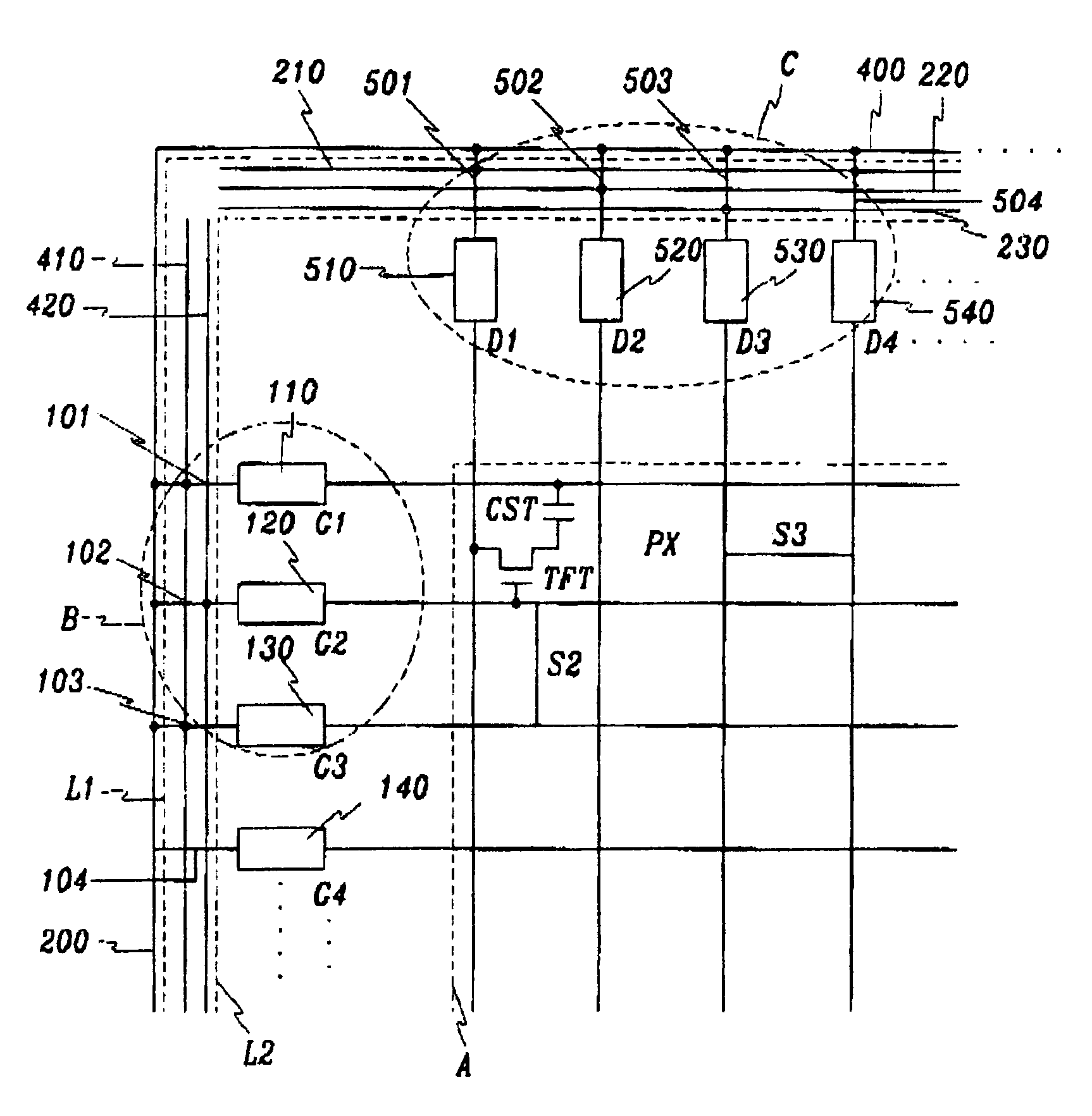
[0071]FIG. 9 is an enlarged layout view of a portion C in FIG. 5, and FIG. 10 is a cross-sectional view taken along line X–X′ in FIG. 9, which specially show the connection of a data shorting bar to a third, a fourth and a fifth secondary line.

[0072]As shown in FIGS. 9 and 10, a third, a fourth and a fifth secondary lines 210, 220 and 230 made of the same metal as a gate wire are formed on a substrate 1 in the horizontal direction, and a gate insulating film 150 is deposited thereon. A data wire 55, including data lines D1, D2, D3 and D4, data pads 510, 520, 530 and 540, data extensions 501, 502, 503 and 504 extending from the data pads and a data shorting bar 400 connected to the data extensions, is formed on the gate insulating film 150. A passivation film 250 is formed thereon.

[0073]Contact holes F, H and J are formed in the passiva...

third embodiment

[0125]FIG. 18 shows testing wave forms to improve this problem.

[0126]In FIG. 18, signals DR, DG and DB applied to R, G and B pixel columns and signals Godd and Geven applied to odd and even gate lines are mostly similar to the signals in the second embodiment. Instead, the signals applied to the R, G and B pixel columns invert with a period of two times the width of the gate pulse.

[0127]Therefore, there is no difficulty in charging the R, G and B signals into the pixels, it is easy to synchronize the gate pulse and the data signals, and the flicker effect is reduced. As a result, the test method according to the third embodiment is superior to test a uniformity and defects under high and off states.


PUM


Abstract

A plurality of gate lines are formed on an insulating substrate in the horizontal direction, a gate shorting bar connected to the data lines is formed in the vertical direction and a gate insulating film is formed thereon. A plurality of data lines intersecting the gate lines are formed on the gate insulating film in the vertical direction, and a data shorting bar connected to the data lines is formed outside the display region. A first shorting bar is formed on the gate insulating film, located between the gate lines and the gate shorting bar, and connected to the odd gate lines. A second secondary shorting bar is formed parallel to the first shorting bar and connected to the even gate lines.

Description

[0001]The present application is a continuation of U.S. patent Ser. No. 09 / 206,317, filed Dec. 7, 1998, and issued as U.S. Pat. No. 6,734,925.BACKGROUND OF THE INVENTION[0002](a) Field of the Invention[0003]The present invention relates to liquid crystal displays (referred as LCDs hereinafter), manufacturing methods thereof and testing methods thereof, in particular, to LCDs having more than two shorting bars, and methods for detecting defects in the LCDs by using the shorting bars.[0004](b) Description of the Related Art[0005]Shorting bars of a liquid crystal display are used to discharge a electrostatic charges which are generated in the manufacturing process of the LCD and to test the LCD after the manufacturing process is completed.[0006]A conventional LCD is described in detail with reference to the accompanying drawings.[0007]FIG. 1 is a schematic diagram of a conventional thin film transistor (referred as TFT hereinafter) substrate for a LCD having shorting bars, FIG. 2 is a ...

Claims


Application Information

Patent Timeline
IPC IPC(8): G01R31/00G02F1/1343G02F1/133G02F1/1345G02F1/136G02F1/1362G02F1/1368G09F9/35H01L21/00
CPCG02F1/1345G02F1/1362G02F1/136286G09G3/006G09G3/3648G02F1/136204G09G2330/08G09G2300/0426G02F2001/136254G02F1/136254
Inventor LEE, SANG-KYOUNGKIM, DONG-GYUMOON, MIN-HYUNG
Owner SAMSUNG DISPLAY CO LTD
Why Eureka
Try Eureka