Clock control of functional units in an integrated circuit based on monitoring unit signals to predict inactivity

a technology of functional units and integrated circuits, applied in instruments, climate sustainability, sustainable buildings, etc., can solve the problems of power and thermal constraints placed on modern semiconductor devices, over-all power consumption within an integrated circuit, and the limiting factor of the performance and functionality of a single device, the more power it typically consumes, and the more power it is typically consumed

Active Publication Date: 2006-01-03
ADVANCED SILICON TECH
View PDF15 Cites 104 Cited by
  • Summary
  • Abstract
  • Description
  • Claims
  • Application Information

AI Technical Summary

Benefits of technology

[0024]Clocking is controlled separately to the integer execution unit and floating point execution unit. The microprocessor includes an integer activity detector unit and a floating-point activity detector unit. These activity detector units correspond to activity detector and clock control units, described above. The integer activity detector unit determines when the integer execution unit will be inactive and shuts off clocking to the integer execution unit when it is inactive. Similarly, the floating-point activity detector unit determines when the floating-point execution unit is inactive and shuts off clocking to the floating-point execution unit during its periods of inactivity. Clocking is reestablished to the integer execution unit and / or floating point execution unit when activity is detected by either the floating-point activity detector unit and / or the integer activity detector unit.

Problems solved by technology

Some of the factors contributing to overall power consumption within an integrated circuit are dynamic power consumption, (power consumption caused by capacitive charging during the switching of a transistor) and static power, (power caused by leakage current through a transistor in the off state).
The power and thermal constraints placed on modern semiconductor devices are rapidly becoming a limiting factor to the performance and functionality available in a single device.
The high clock speeds are to drive the integrated circuit faster to perform its respective job faster, and the faster the integrated circuit operates the more the more power it typically consumes.
If the heat is not efficiently dissipated, then the semiconductor material that makes up the integrated circuit may continue to increase in temperature which could lead to malfunction, device damage, thermal runaway, etc.
Thermal runaway is where the device will continue to increase in heat and power consumption until it eventually and permanently fails.
Thermal problems may lead to actual breakdown of one or more of the device junctions in the semiconductor material.
The more semiconductor devices that are contained in an integrated circuit for example, the greater the power consumption and need for efficient heat dissipation.
Even with all of the technological advances made in integrated circuits, problems still arise from an increasing need to miniaturize and increase the density in already crowded semiconductor die.
Thus, lower power requirements lead to smaller power supplies.
If power consumption and heat related problems cannot be addressed, a device may have to be operated at a lower frequency or at a lower voltage or include fewer devices than desired to reduce power consumption and avoid thermal problems.
Excessive heat also affects the characteristics of other non-silicon materials used in the design and assembly of electronic equipment today.
Due to cost-reducing steps that may be taken, some materials that are used in today's equipment may not withstand the excessive heat generated within that equipment.
For example, certain types of plastic, rubber, vinyl, and adhesive may deteriorate and / or warp when exposed to excessive heat, possibly affecting the fit, form or functionality of the equipment.
Thus, there is a need to dissipate heat faster and lower the average operating temperature of a device.
These techniques may solve some of the problem, but may not lend themselves to every application.
Although enlarging the leads on an IC may provide some heatsink capability, this technique may not apply to all package types and there are physical limitations to the size the leads may be.
However, heatsinks and fans generally take up valuable space and add cost in a system.
These devices may not be cost effective in some designs where cost is an issue.
Many conventional power management techniques may become inadequate in designs where space constraints are present within the equipment.
Power consumption may become more of an issue because of the physical size of the power supply and battery life.
While this technique may be effective, it may only be feasible in some applications.
However, performance goals may not be met at a lower frequency.
Even though this type of sacrifice reduces power consumption, it may result in a design that does not meet performance and functionality goals.

Method used


Image

  • Clock control of functional units in an integrated circuit based on monitoring unit signals to predict inactivity
  • Clock control of functional units in an integrated circuit based on monitoring unit signals to predict inactivity
  • Clock control of functional units in an integrated circuit based on monitoring unit signals to predict inactivity

Examples


Embodiment Construction

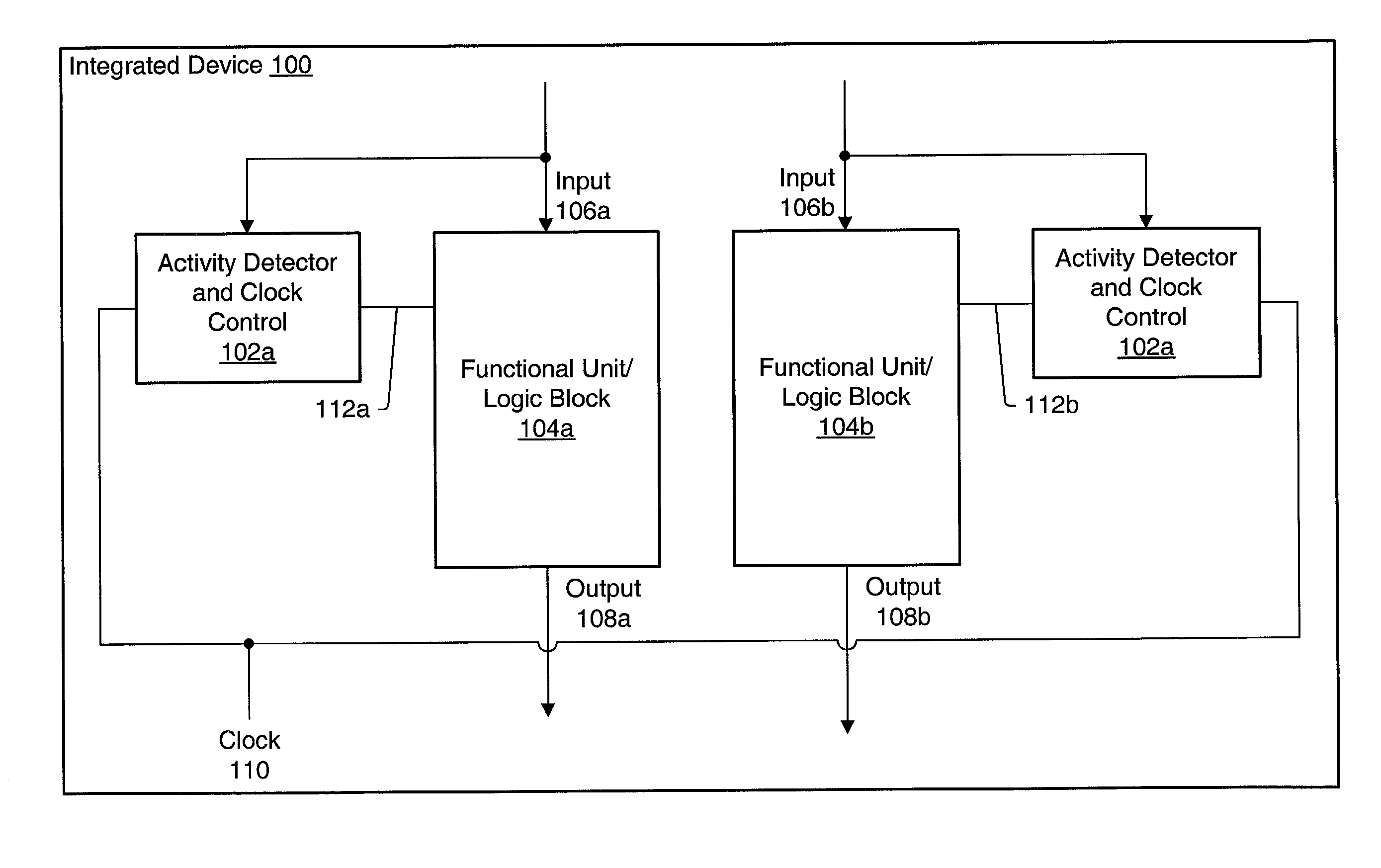
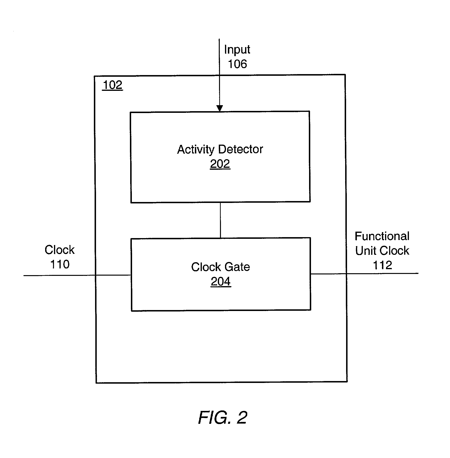
[0033]FIG. 1 illustrates a semiconductor device or integrated circuit 100 having separate clock control for a number of different functional units or logic blocks 104, according to one embodiment. The device 100 includes a number of different functional units or logic blocks 104. Each functional unit 104 receives one or more input signals 106 and produces one or more outputs 108. A functional unit may be a section of circuitry or other logic structure within the integrated circuit 100 that perform a particular function or task. Each function unit 104 represents a portion of the integrated circuit 100 that is not always active. For example, while functional unit 104a is operating on input 106a to produce output 108a, functional unit 104b may be inactive, and vice versa. In some instances function unit 104a and 104b may both be inactive or both be active. Note that while FIG. 1 only illustrates two functional units 104a and 104b, integrated circuit device 100 may have more than two fu...


PUM


Abstract

An integrated circuit may have separate clock control for a number of different functional units. Ancillary to some of the functional units may be an activity detector and clock control unit which monitors input to its functional unit to determine when the functional unit will be inactive. When an activity detector and clock control unit determines that a particular functional unit is or will be inactive, it may disable clocking to its functional unit while the functional unit is inactive. When activity detector and clock control unit determines that activity will resume for its functional unit, it enables clocking to its functional unit. Thus, the activity detector and clock control unit for each such functional unit functions to control clocking to its respective functional unit so that during periods of inactivity, inactive functional units are not clocked to reduce the overall static and/or dynamic power consumption for the integrated device.

Description

BACKGROUND OF THE INVENTION[0001]1. Field of the Invention[0002]This invention relates to power management within integrated circuits, and more particularly to monitoring activity for different functional units of an integrated circuit for power management.[0003]2. Description of the Related Art[0004]Some of the factors contributing to overall power consumption within an integrated circuit are dynamic power consumption, (power consumption caused by capacitive charging during the switching of a transistor) and static power, (power caused by leakage current through a transistor in the off state). The power and thermal constraints placed on modern semiconductor devices are rapidly becoming a limiting factor to the performance and functionality available in a single device. VLSI (Very Large Scale Integration) and extreme high clock speeds have become the norm. The high clock speeds are to drive the integrated circuit faster to perform its respective job faster, and the faster the integr...

Claims


Application Information

Patent Timeline
Patent Type & Authority Patents(United States)
IPC IPC(8): G06F1/32
CPCG06F1/3203G06F1/3215G06F1/3287G06F1/3237G06F9/3869G06F1/325G06F9/3836Y02B60/1221Y02B60/1278Y02B60/1282Y02D10/00
Inventor FILIPPO, MICHAEL A.
Owner ADVANCED SILICON TECH
Why Eureka
Try Eureka