Electronic devices with small functional elements supported on a carrier

a technology of functional elements and electronic devices, applied in the direction of non-printed jumper connection addition, printed circuit non-printed electric components association, instruments, etc., can solve the problems of high cost of assembling functional components into other substrates, high cost of end product, and high cost of manufacturing of rf id tags

Inactive Publication Date: 2006-01-10
RUIZHANG TECH LTD CO
View PDF87 Cites 95 Cited by
  • Summary
  • Abstract
  • Description
  • Claims
  • Application Information

AI Technical Summary

Problems solved by technology

The growth for the use of functional components, however, has been inhibited by the high cost of assembling the functional components into other substrates.
Often the assembling of these components requires complex and multiple processes thereby causing the price of the end product to be expensive.
Further, the manufacturing of these RF ID tag is costly because of inefficient and wasteful use of the technologies and the materials used to make these products under the current method.
Depositing semiconductor chips and other components onto substrates having the antenna is complex and tedious.
Because the semiconductor chips need to be large, material costs are thus high.
Further, if there is a defective chip, the whole RF ID tag would be defective and would not be discovered until the whole assembly is complete.
This is intrinsically wasteful and inefficient.
Making LCDs has become increasingly difficult because it is challenging to produce LCDs with high yields.
Furthermore, the packaging of driver circuits has become increasingly difficult as the resolution of the LCD increases.
The packaged driver elements are also relatively large and occupy valuable space in a product, which results in larger and heavier products.
Furthermore, large displays such as those for signage purposes are expensive to make.
Large displays are often made out of material with large-feature-size patterns that must be connected to integrated circuits (ICs) with small feature sizes. the This results in expensive packages that are bulky and expensive.
These chip carriers, such as leaded chip packages, Tape Automated Bonded (TAB) carrier or flip chip carriers are bulky and expensive.

Method used


Image

  • Electronic devices with small functional elements supported on a carrier
  • Electronic devices with small functional elements supported on a carrier
  • Electronic devices with small functional elements supported on a carrier

Examples


Embodiment Construction

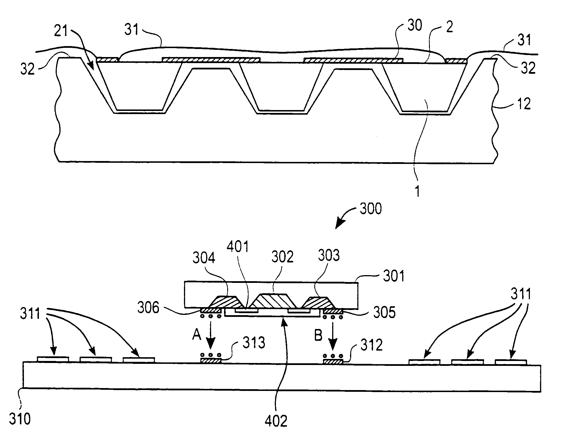
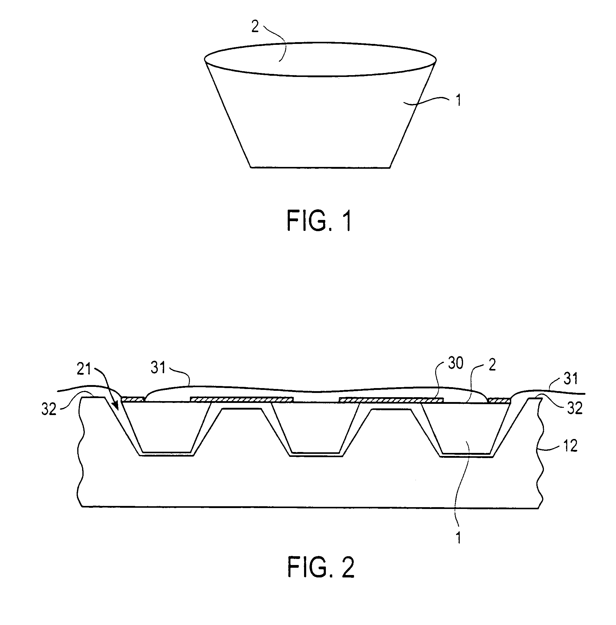
[0020]FIG. 1 illustrates an exemplary embodiment of an object that is functional component block 1. Block 1 has a top surface 2 upon which a circuit element is situated (not shown). The circuit element on the top surface 2 may be an ordinary integrated circuit (IC) for any particular function. For example, the IC may be designed to drive a pixel of a display. The IC may also be designed to receive power from another circuit for the operation of a passive RF ID tag. Alternatively, the IC may be designed to receive power from an energy source (e.g. battery) for the operation of an active RF ID tag. In one embodiment, block 1 has a trapezoidal cross-section where the top of the block is wider than the bottom of the block 1. Block 1 may be created from a host substrate and separated from this substrate. This method of making block 1 can be found in the method described in copending U.S. patent application Ser. No. 09 / 251,220 now U.S. Pat. No. 6,291,896 referenced above. This patent is h...


PUM

PropertyMeasurementUnit
width×lengthaaaaaaaaaa
sizeaaaaaaaaaa
sizeaaaaaaaaaa

Abstract

Methods and apparatuses for an electronic assembly. The electronic assembly has a first object created and separated from a host substrate. The first object has a first electrical circuitry therein. A carrier substrate is coupled to the first object wherein the first object is being recessed below a surface of the carrier substrate. The carrier substrate further includes a first carrier connection pad and a second carrier connection pad that interconnect with the first object using metal connectors. A receiving substrate, which is substantially planar, including a second electrical circuitry, a first receiving connection pad, and a second receiving connection pad that interconnect with the second electrical circuitry using the metal connectors. The carrier substrate is coupled to the receiving substrate using the connection pads mentioned.

Description

RELATED APPLICATIONS[0001]This is a divisional of U.S. patent application Ser. No. 10 / 464,031, now U.S. Pat. No. 6,816,380, filed on Jun. 17, 2003, which is a continuation of U.S. patent application No. 09 / 872,985, filed on May 31, 2001, now U.S. Pat. No. 6,606,247.FIELD OF THE INVENTION[0002]The present invention relates generally to the field of fabricating electronic devices with small functional elements depositing in various substrates and apparatuses comprising these electronic devices.BACKGROUND OF THE INVENTION[0003]There are many examples of functional elements or components which can provide, produce, or detect electromagnetic signals or other characteristics. An example of using the functional components is using them as an array of a display drivers in a display where many pixels or sub-pixels are formed with an array of electronic elements. For example, an active matrix liquid crystal display includes an array of many pixels or sub-pixels which are fabricated using amor...

Claims


Application Information

Patent Timeline
Patent Type & Authority Patents(United States)
IPC IPC(8): H05K1/11H05K1/14H05K7/02G06K19/07G06K19/077H01L29/06H05K1/18H05K3/22H05K3/32
CPCG06K19/07749G06K19/07752G06K19/07779G06K19/07783H01L24/24H01L24/82H01L24/95H01L24/96H01Q1/2208H01Q7/00H05K1/141H05K3/222G06K19/0775Y10T29/49204H01L29/0657H01L2224/24137H01L2224/24227H01L2224/95085H01L2924/01013H01L2924/01015H01L2924/01027H01L2924/01029H01L2924/01047H01L2924/01049H01L2924/01075H01L2924/01079H01L2924/01082H01L2924/10158H01L2924/14H01L2924/15153H01L2924/15155H01L2924/15165H01L2924/19041H01L2924/19042H01L2924/19043H01L2924/30105H05K1/183H05K3/321H05K2201/10477Y10T29/49018Y10T29/4913Y10T29/49002H01L2924/01005H01L2924/01006H01L2924/01033H01L2924/01087H01L2924/12041Y10T29/49117Y10T29/49016H01L2924/12044H01L2224/95136H01L2924/00
Inventor CREDELLE, THOMAS LLOYDGENGEL, GLENNSTEWART, ROGER GREENJOSEPH, WILLIAM HILL
Owner RUIZHANG TECH LTD CO
Why Eureka
Try Eureka