Reaction mass for a stage device

a stage device and reaction mass technology, applied in the direction of shock absorbers, instruments, printers, etc., can solve the problems of affecting the photolithography system, the difficulty of accurately aligning the overlay of circuit patterns of multi-layered integrated circuits, and the impact of vibration on the photolithography system, so as to reduce the impact force

Inactive Publication Date: 2006-01-17
NIKON CORP
View PDF12 Cites 9 Cited by
  • Summary
  • Abstract
  • Description
  • Claims
  • Application Information

AI Technical Summary

Benefits of technology

[0018]Yet a further aspect of the present invention is a method for reducing a vibration force transmitted by a base to a stationary surface. The method comprises the steps of supporting the base and levitating the base above the stationary surface so that the base can move relative to the stationary surface, and controlling movement of the base in at least one degree of freedom, the movement being caused by a disturbance force.

Problems solved by technology

As the miniaturization of a circuit pattern progresses, the focus depth of the projection exposure apparatus becomes very small, making it difficult to align accurately the overlay of circuit patterns of the multi-layered integrated circuit.
Since both the reticle base and wafer stage base are rigidly connected to the apparatus frame of the exposure apparatus, the reaction forces are transmitted to the apparatus frame and the ground, causing a detrimental vibration to the photolithography system.

Method used


Image

  • Reaction mass for a stage device
  • Reaction mass for a stage device
  • Reaction mass for a stage device

Examples


Embodiment Construction

[0034]Reference will now be made in detail to an embodiment of the apparatus, system, and method consistent with the principles of the present invention, examples of which are illustrated in the accompanying drawings. The invention will be further clarified by the following examples, which are intended to be exemplary of the invention.

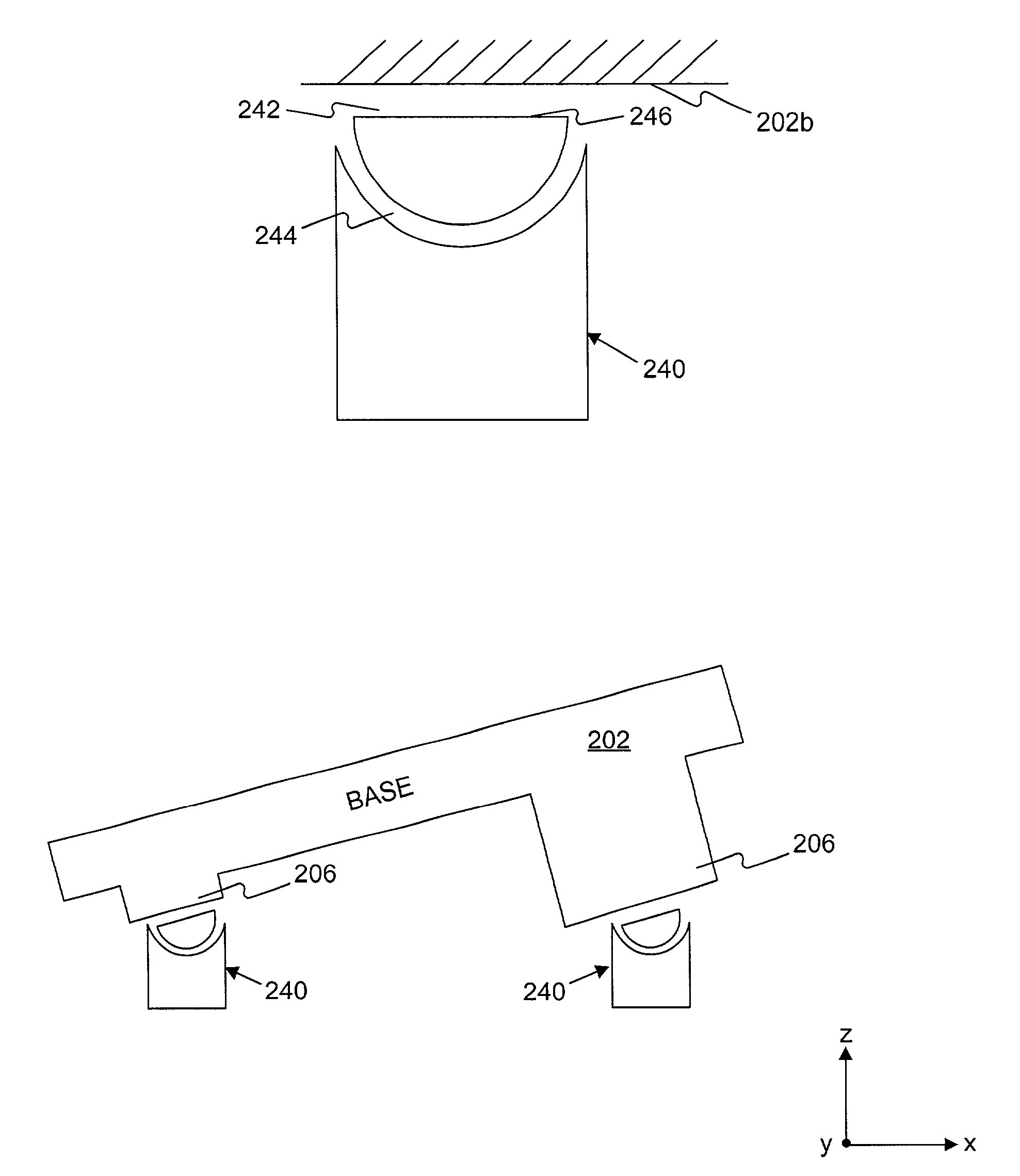
[0035]The apparatus, system, and method consistent with the principles of the present invention are useful to minimize forces transmitted from a moving object, such as a wafer stage assembly of a photolithography system, to a stationary surface, such as the ground or an exposure apparatus frame. Therefore, vibrations from the wafer stage assembly to other parts of the photolithography system can be prevented. The principles of this invention are similarly applicable to other parts of the photolithography system, such as a reticle stage assembly. Thus, this invention is not limited to any particular application. Rather, the stage assembly, support syste...


PUM

PropertyMeasurementUnit
of wavelengthaaaaaaaaaa
reaction forceaaaaaaaaaa
distancesaaaaaaaaaa

Abstract

A stage assembly and support system are provided to stabilize a stage base, such as a wafer stage base or a reticle stage base, minimizing forces transmitted from the stage assembly to a stationary surface, such as the ground, and thereby preventing vibration of other parts or systems in a wafer manufacturing process. Depending of the applicable photolithography system, a reticle stage and / or a wafer stage are accelerated in response to a wafer manufacturing control system to position the semiconductor substrates. The jerking motions of the reticle stage and / or wafer stage cause reaction forces acting on the reticle stage base and / or wafer stage base. The reaction forces induce vibration to the stationary surface and surrounding parts of the photolithography system. The wafer stage assembly and support system according to this invention allow the reticle stage base and / or wafer stage base to move relative the stationary surface. The base, acting as a massive reaction mass, stores a kinetic energy from the reaction force and gradually dissipates such energy by applying small forces to the reaction mass. The stage assembly and support system according to this invention are also capable of canceling any disturbance forces acting on the base.

Description

BACKGROUND OF THE INVENTION[0001]1. Field of the Invention[0002]This invention relates to a stage assembly, a support system, and method for stabilizing the stage assembly in a photolithography process to manufacture semiconductor wafers. More particularly, this invention relates to the stage assembly, support system, and method for stabilizing the stage assembly to prevent ground vibration.[0003]2. Description of the Related Art[0004]In manufacturing integrated circuits using photolithography, light is transmitted through non-opaque portions of a pattern on a reticle, or photomask, through a projection exposure apparatus, and onto a wafer of specially-coated silicon or other semiconductor material. The uncovered portions of the coating, that are exposed to light, are cured. The uncured coating is then removed by an acid bath. Then, the layer of uncovered silicon is altered to produce one layer of the multi-layered integrated circuit. Conventional systems use visible and ultraviolet...

Claims


Application Information

Patent Timeline
Patent Type & Authority Patents(United States)
IPC IPC(8): G03B27/58G02B27/42F16F7/10G03F7/20
CPCF16F7/1005G03F7/70766G03F7/70716
Inventor YUAN, BAUSANBINNARD, MICHAEL
Owner NIKON CORP
Why Eureka
Try Eureka