Supercharge Your Innovation With Domain-Expert AI Agents!

Electron-beam writing device and electron-beam writing method

a technology of electron beam and writing device, applied in the field of electron beam writing technology, can solve the problems of inability to obtain high positional accuracy, inability to write fast, and inability to achieve high positional accuracy, etc., and achieve the effect of high speed

Inactive Publication Date: 2006-01-24
KONICA MINOLTA INC +1
View PDF3 Cites 1 Cited by
  • Summary
  • Abstract
  • Description
  • Claims
  • Application Information

AI Technical Summary

Benefits of technology

[0020]The present invention is to solve the above problems, and it is an object thereof to provide an electron-beam writing device and an electron-beam writing method, which enable the high-precision, high-speed writing of a line from its writing start position to end position.

Problems solved by technology

To this end, more bits are required, causing a problem that the writing speed is inevitably decreased.
To this end, the number of bits has to be reduced, causing a problem that high positional accuracy cannot be obtained.
Further, when the endpoint of a line segment is calculated in the above-mentioned manner, there is a further problem that causes an endpoint error ΔL806.
This is why the endpoint error 806 is inevitably caused.

Method used


Image

  • Electron-beam writing device and electron-beam writing method
  • Electron-beam writing device and electron-beam writing method
  • Electron-beam writing device and electron-beam writing method

Examples


Embodiment Construction

[0034]The present invention will now be described with reference to FIGS. 3 through 9.

[0035](Structure of Electron-Beam Writing Device)

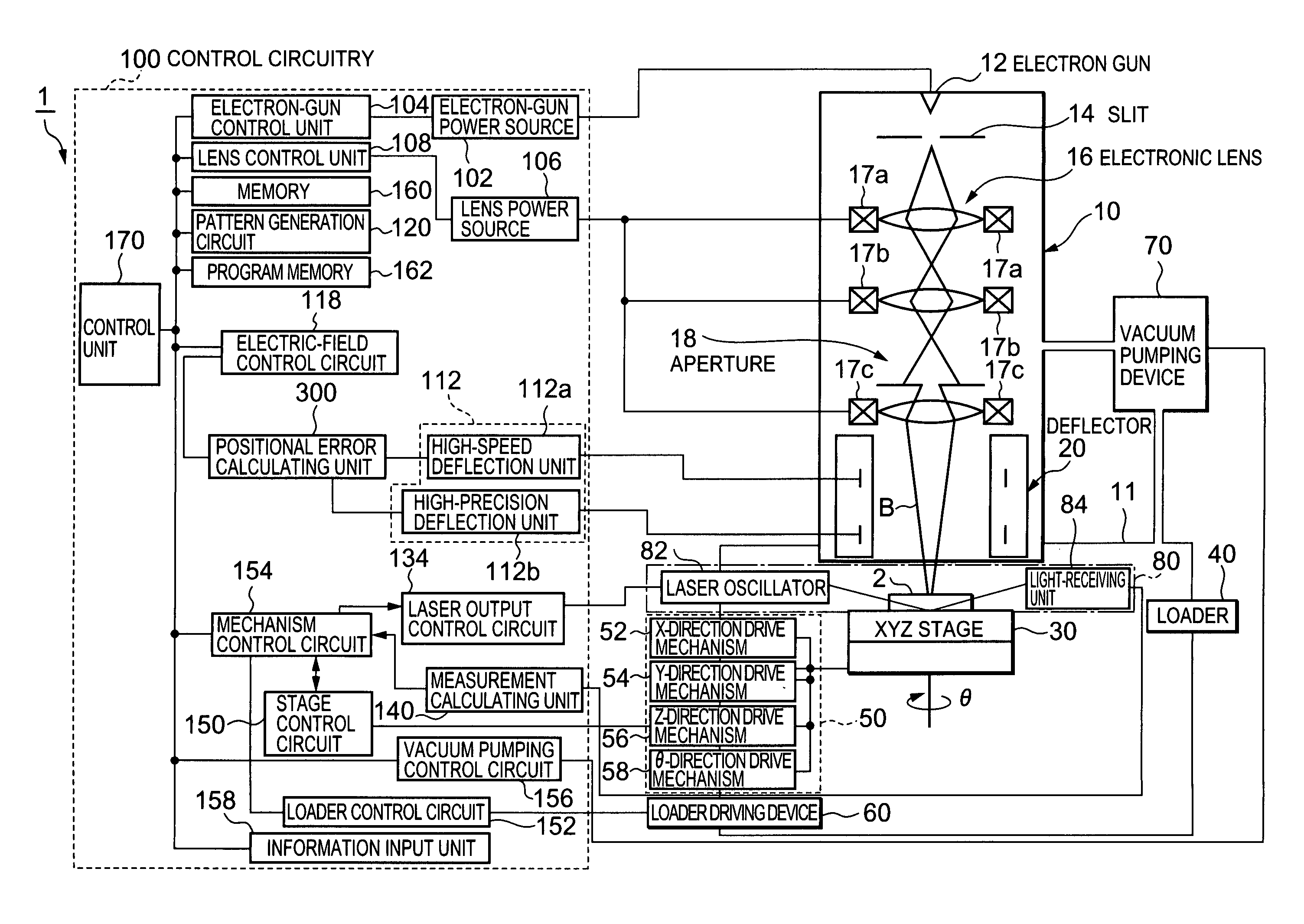
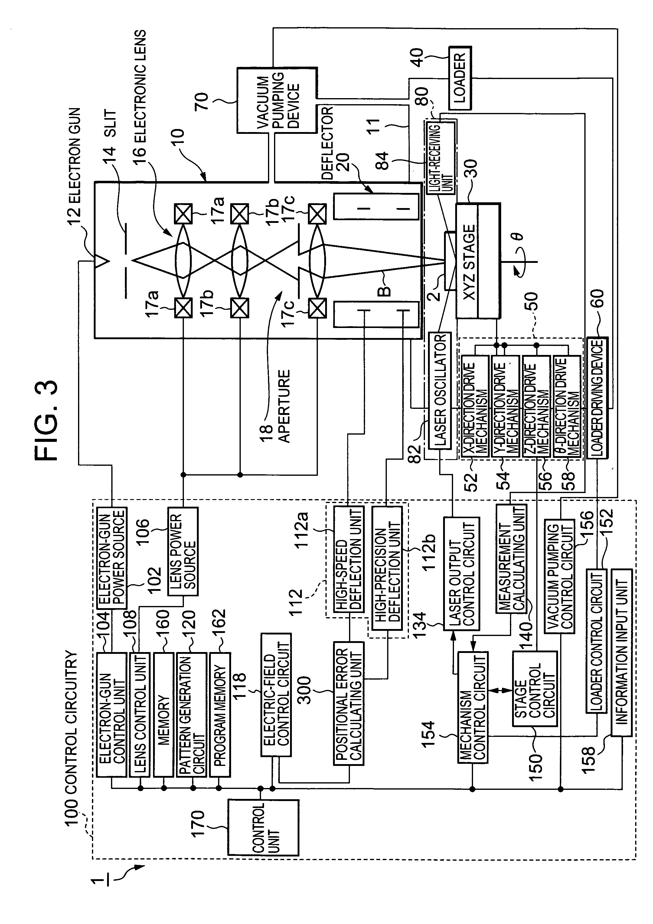
[0036]FIG. 3 is a schematic diagram showing the general structure of an electron-beam writing device according to the embodiment. The electron-beam writing device 1 forms a high-current, high-resolution electron-beam probe for scanning a target substrate 2 at high speed. The device includes an electron gun 12 as electron-beam generating means that forms the high-resolution electron-beam probe to generate and irradiate an electron beam to the target, a slit 14 through which the electron beam from the electron gun 12 passes, electronic lenses 16 for controlling the focal position of the electron beam passing through the slit 14 on the substrate 2, an aperture 18 arranged in a path along which the electron beam is irradiated, and a deflector 20 for deflecting the electron beam to control the scanning position and the like of the target substrate 2. Thes...


PUM

PropertyMeasurementUnit
lengthaaaaaaaaaa
distanceaaaaaaaaaa
resolving poweraaaaaaaaaa

Abstract

The present invention aims at providing a device and method for writing a line with a high degree of precision at high speed. Distance calculation means 311 calculates the start-to-end point distance L of a writing pattern (S502), and number-of-scan-clocks calculating means 312 calculates the number of scan clocks required to write the writing pattern based on the start-to-end point distance L and a unit distance corresponding to the minimum time resolution for a high-speed D / A converter 306 (S503). Count conversion means 605 separates the start-to-end point distance L into X and Y components to convert them in an equation using the number of scan clocks (S504). Based on the equation, variable rate calculating means 314 calculates an extinction ratio to determine the extinction ratio at a variable attenuator 307 (S505). ATT D / A converter 303 specifies the extinction ratio at the attenuator 307 to reduce the unit distance corresponding to the resolving power of the high-speed D / A converter 306 so that an electron beam will be irradiated and scanned at intervals of the reduced unit distance to perform writing.

Description

BACKGROUND OF THE INVENTION[0001]1. Field of the Invention[0002]The present invention relates to electron-beam writing technology, and particularly to a technique for high-precision, high-speed writing.[0003]2. Description of the Prior Art[0004]In recent years, attempts have been made to perform writing using an electron-beam writing device (for example, see Japanese patent laid-open No. 273583 / 1996 (Hei 8-273583)). A predetermined pattern is written by such an electron-beam writing device in which a deflector deflects an electron beam so that the electron beam will be scanned over the surface of a target substrate material. The deflector typically consists of two units, i.e. a high-precision deflection unit and a high-speed deflection unit. The high-precision deflection unit specifies the position of a target area (hereinafter called a writing field), and the high-speed deflection unit deflects the electron beam within the writing field so that the electron beam will be scanned to ...

Claims


Application Information

Patent Timeline
Patent Type & Authority Patents(United States)
IPC IPC(8): H01J37/28H01J37/256G11C5/00H01J37/302H01J37/304H01J37/317
CPCB82Y10/00B82Y40/00H01J37/3045H01J37/3174H01J37/3026H01J2237/31761
Inventor MASUDA, OSAMUFURUTA, KAZUMIHAYASHI, KUNITOKOBAYASHI, KAZUHIKO
Owner KONICA MINOLTA INC
Features
  • R&D
  • Intellectual Property
  • Life Sciences
  • Materials
  • Tech Scout
  • Unparalleled Data Quality
  • Higher Quality Content
  • 60% Fewer Hallucinations
Learn More