Method and apparatus for creating imaging recipe

a technology of imaging recipe and apparatus, applied in the field of methods and apparatus for creating imaging recipe, can solve the problems of difficult setting of simulation parameters and inability to select appropriate imaging points

Active Publication Date: 2009-07-07
HITACHI HIGH-TECH CORP
View PDF26 Cites 40 Cited by
  • Summary
  • Abstract
  • Description
  • Claims
  • Application Information

AI Technical Summary

Benefits of technology

[0009]The present invention relates to an apparatus and method designed to create an imaging recipe (including: coordinates of imaging points, imaging conditions, and image template information) for evaluating shapes of patterns by measuring electrical wiring widths and other various dimension values of the patterns from observation images. In the above apparatus and method, analysis using CAD images converted from CAD data can create (generate) the imaging recipe automatically and within a minimum time.
[0012]In addition, the CAD image creation unit in the above aspect of the present invention includes an image-quantizing width determination section which creates the above CAD images by converting the above CAD data into image form by use of the image-quantizing width determined from the CAD data on the basis of reference pattern width to be noted. In the image-quantizing width determination section, the reference pattern width to be noted includes a minimum line width or minimum inter-pattern distance of the semiconductor patterns to be noted. Furthermore, the CAD image-creation unit in the above aspect of the present invention is constructed so that the minimum line width or minimum inter-pattern distance of the semiconductor patterns is either calculated from the CAD data automatically, assigned by a user, or calculated from the CAD data automatically on the basis of user-set parameters (conditions). Besides, the above reference pattern width has its value specified in a header (or the like) of the CAD data or displayed in GUI (Graphic User Interface) screen mode. Moreover, if the reference pattern width differs between the CAD data regions extracted, the CAD data is converted into image form with image-quantizing widths different for each of the extracted CAD data regions. Determining image-quantizing widths in this way prevents an image size from becoming redundant and makes it possible to generate the CAD images that have held a pattern structure to be noted.
[0014]According to the present invention, automatic determination of imaging points (including a part or all of an addressing point, focusing point, stigmatism control point, brightness and contrast control point, or end measuring point) or the like from the CAD image is possible by using a CAD image that has been created based on image-quantizing width, assigned brightness, geometrical deformation, and / or the like, for which reason, the imaging creation that has conventionally been manually conducted can be implemented more easily and at higher speed.
[0015]According to the present invention, during actual observation of imaging points through a SEM, it is also possible to match a CAD image (template) whose coordinates are known and a SEM image very accurately, and consequently to evaluate a shape and dimensions of a pattern very accurately.

Problems solved by technology

Therefore, there has been the problem that appropriate imaging points cannot be selected because of a significant difference in visual or apparent position between the above linear image and an actual SEM image.
In addition, these simulation parameters are not easy to set.

Method used


Image

  • Method and apparatus for creating imaging recipe
  • Method and apparatus for creating imaging recipe
  • Method and apparatus for creating imaging recipe

Examples


Embodiment Construction

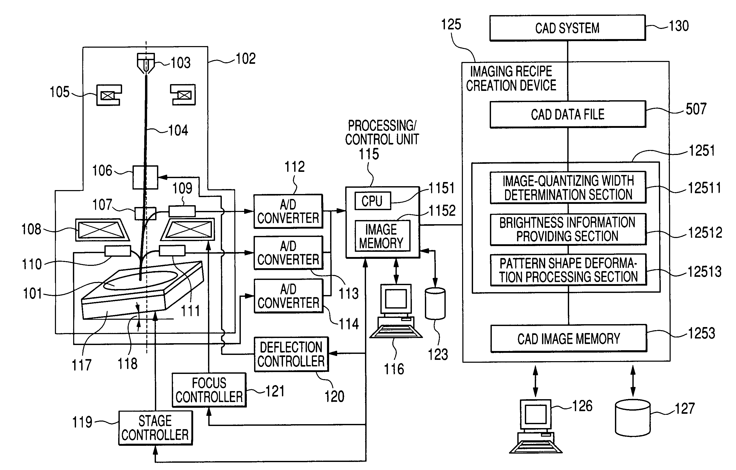
[0042]Embodiments of a SEM apparatus with an imaging recipe creation function according to the present invention, namely, a semiconductor pattern shape evaluation apparatus using a scanning electron microscope such as a critical-dimension scanning electron microscope (CD-SEM), will be described hereunder using FIGS. 1 to 25.

[0043]Factors such as decreases in design margins, coupled with further fineness and high density of LSI patterns, are substantially increasing the number of sections to be inspected to dimensionally manage semiconductor patterns. These tendencies are bringing about a strong demand for the improvement of the throughputs and automation ratios of the SEM apparatuses and other apparatuses used as dimensional management tools.

[0044]To use a SEM apparatus (or the like) to observe measuring points as dimensionally critical points on the semiconductor patterns to be inspected, and evaluate the shapes of these patterns by measuring the wiring widths and other various dim...


PUM


Abstract

In an imaging recipe creating apparatus that uses a scanning electron microscope to create an imaging recipe for SEM observation of a semiconductor pattern, in order that the imaging recipe for measuring the wiring width and other various dimension values of the pattern from an observation image and thus evaluating the shape of the pattern is automatically generated within a minimum time by the analysis using the CAD image obtained by conversion from CAD data, an CAD image creation unit that creates the CAD image by converting the CAD data into an image format includes an image-quantizing width determining section, a brightness information providing section, and a pattern shape deformation processing section; the imaging recipe being created using the CAD image created by the CAD image creation unit.

Description

BACKGROUND OF THE INVENTION[0001]The present invention relates to a method and apparatus for creating imaging recipe used to acquire images at any position on a sample with a critical-dimension scanning electron microscope (CD-SEM) or the like. The imaging recipe defines not only coordinates of imaging points of addressing point and evaluation point (end measuring point), but also the image templates or imaging conditions (or the like) that are associated with the above coordinates. The invention is also concerned with an apparatus (SEM apparatus) for evaluating shapes of patterns formed on semiconductor wafers.[0002]Traditionally, CD-SEMs and the like are most commonly used to inspect the workmanship of the highly accurate wiring patterns formed on semiconductor wafers. In SEM apparatuses such as the CD-SEMS, dimensionally critical points on the semiconductor patterns to be inspected are observed as measuring points through the SEM, then various dimensional data on the patterns, su...

Claims


Application Information

Patent Timeline
Patent Type & Authority Patents(United States)
IPC IPC(8): G06F17/50G06K9/00
CPCG03F7/70625
Inventor MIYAMOTO, ATSUSHINAGATOMO, WATARUMATSUOKA, RYOICHIMOROKUMA, HIDETOSHISUTANI, TAKUMICHI
Owner HITACHI HIGH-TECH CORP
Why Eureka
Try Eureka