Dual-port SRAM in a programmable logic device

a programmable logic and integrated circuit technology, applied in logic circuits, digital storage, instruments, etc., can solve the problems of increasing complexity of programmable logic integrated circuits such as pals, plds, fpgas, etc., and achieve the effect of efficient and effective implementation of read-during-write features

Inactive Publication Date: 2006-01-31
ALTERA CORP
View PDF3 Cites 15 Cited by
  • Summary
  • Abstract
  • Description
  • Claims
  • Application Information

AI Technical Summary

Benefits of technology

[0006]The present invention provides circuitry and techniques for efficiently and effectively implementing a read-during-write feature for memory blocks. In a specific embodiment, the memory blocks are the dual-port SRAM memory blocks of a programmable logic integrated circuit.

Problems solved by technology

Programmable logic integrated circuits such as PALs, PLDs, FPGAs, LCAs, and others are becoming more complex and continually evolving to provide more user-programmable features on a single integrated circuit.

Method used


Image

  • Dual-port SRAM in a programmable logic device
  • Dual-port SRAM in a programmable logic device
  • Dual-port SRAM in a programmable logic device

Examples


Embodiment Construction

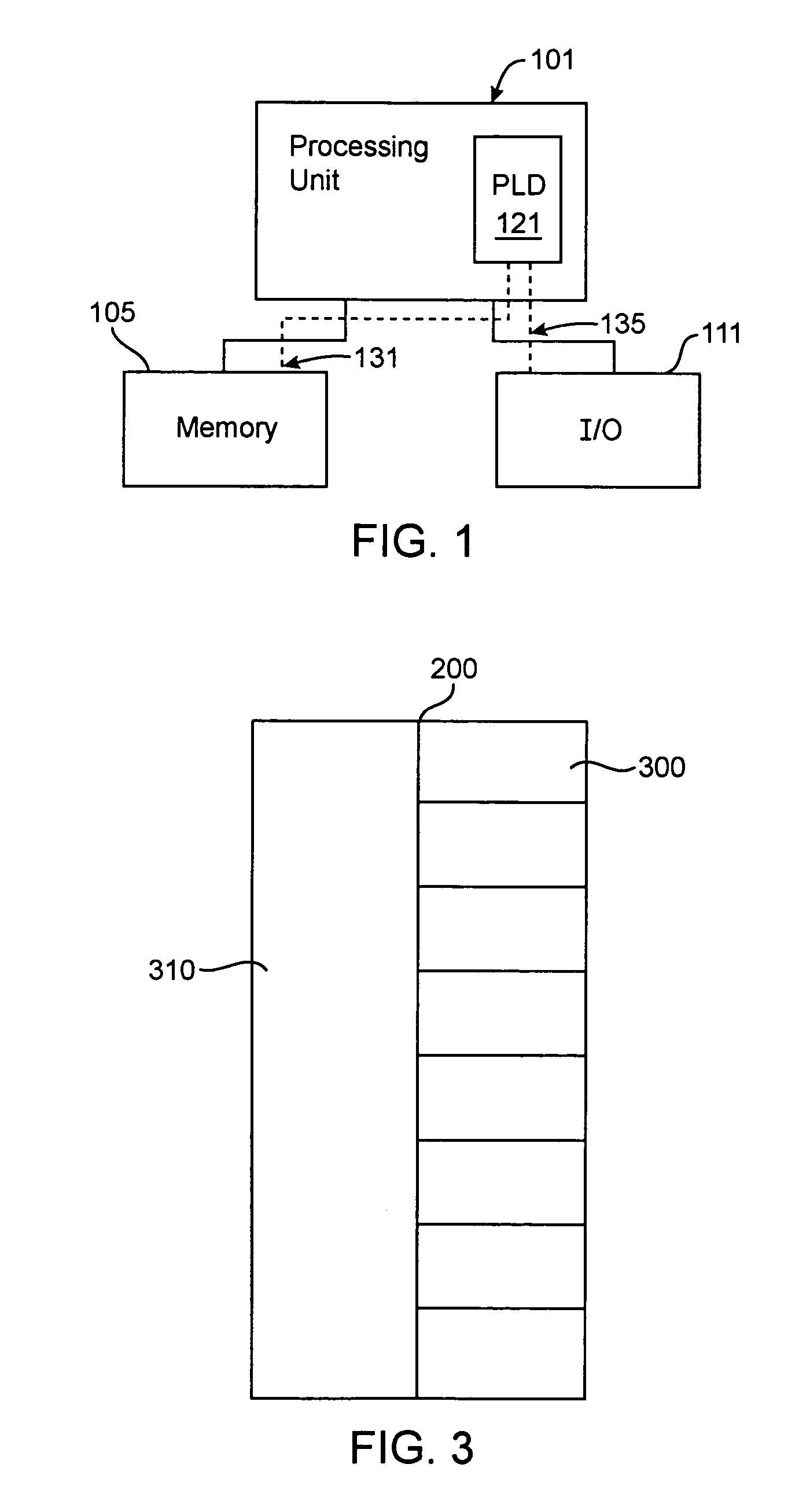
[0030]FIG. 1 shows a block diagram of a digital system within which the present invention may be embodied. The system may be provided on a single board, on multiple boards, or even within multiple enclosures. FIG. 1 illustrates a system 101 in which a programmable logic device 121 may be utilized. Programmable logic devices or programmable logic integrated circuits are sometimes referred to as a PALs, PLAs, FPLAs, PLDs, CPLDs, EPLDs, EEPLDs, LCAs, or FPGAs and are well-known integrated circuits that provide the advantages of fixed integrated circuits with the flexibility of custom integrated circuits. Such devices allow a user to electrically program standard, off-the-shelf logic elements to meet a user's specific needs. See, for example, U.S. Pat. No. 4,617,479, incorporated by reference for all purposes. Programmable logic devices are currently represented by, for example, Altera's MAX®, FLEX®, and APEX™ series of PLDs. These are described in, for example, U.S. Pat. Nos. 4,871,930...


PUM


Abstract

Methods and apparatus for a dual-port SRAM in a programmable logic device. One embodiment provides a programmable logic integrated circuit including a dual-port memory. The memory includes a plurality of memory storage cells, and each memory storage cell has a memory cell having a first node and a second node, a first series of devices connected between a first data line and the first node of the memory cell, and a second series of devices connected between a second data line and the second node of the memory cell. A read cell is connected to the second node of the memory cell. A word line is connected to a first device in the first series of devices, a second device in the second series of devices, and the read cell.

Description

CROSS-REFERENCES TO RELATED APPLICATIONS[0001]This application is a divisional application of U.S. patent application Ser. No. 09 / 883,087, filed Jun. 15, 2001, now U.S. Pat. No. 6,661,733 issued on Dec. 09, 2003 which claims the benefit of U.S. provisional patent application 60 / 211,936, filed Jun. 15, 2000, both or which are incorporated by reference.BACKGROUND OF THE INVENTION[0002]The present invention relates to the field of integrated circuits and in particular, to a dual-port memory within a programmable logic integrated circuit.[0003]Programmable logic integrated circuits such as PALs, PLDs, FPGAs, LCAs, and others are becoming more complex and continually evolving to provide more user-programmable features on a single integrated circuit. Modern programmable logic integrated circuits incorporate programmable logic including logic gates, products terms, or look-up tables. Programmable logic integrated circuits also include embedded user-programmable memory or RAM.[0004]Despite ...

Claims


Application Information

Patent Timeline
Patent Type & Authority Patents(United States)
IPC IPC(8): G11C8/00G11C8/16H03K19/177
CPCH03K19/1776G11C8/16
Inventor PAN, PHILIP Y.SUNG, CHIAKANGHUANG, JOSEPHWANG, BONNIENGUYEN, KHAIWANG, XIAOBAORANGAN, GOPINATHKIM, IN WHANCHONG, YAN
Owner ALTERA CORP
Why Eureka
Try Eureka