Image display device and adjustment for alignment

a technology which is applied in the field of image display device and adjustment for alignment, can solve the problems of further reduction and limit of the depth dimension of the device, and achieve the effect of reducing the depth dimension

Inactive Publication Date: 2006-02-07
MITSUBISHI ELECTRIC CORP
View PDF46 Cites 42 Cited by
  • Summary
  • Abstract
  • Description
  • Claims
  • Application Information

AI Technical Summary

Benefits of technology

[0014]It is therefore an object of the present invention to provide an image display device that provides an enlarged display of distortion-free images and permits further reduction of its depth dimension than in the prior art.

Problems solved by technology

The conventional device configurations described above impose limitations on the reduction of the depth dimension of the device and permit no further reduction.

Method used


Image

  • Image display device and adjustment for alignment
  • Image display device and adjustment for alignment
  • Image display device and adjustment for alignment

Examples


embodiment 1

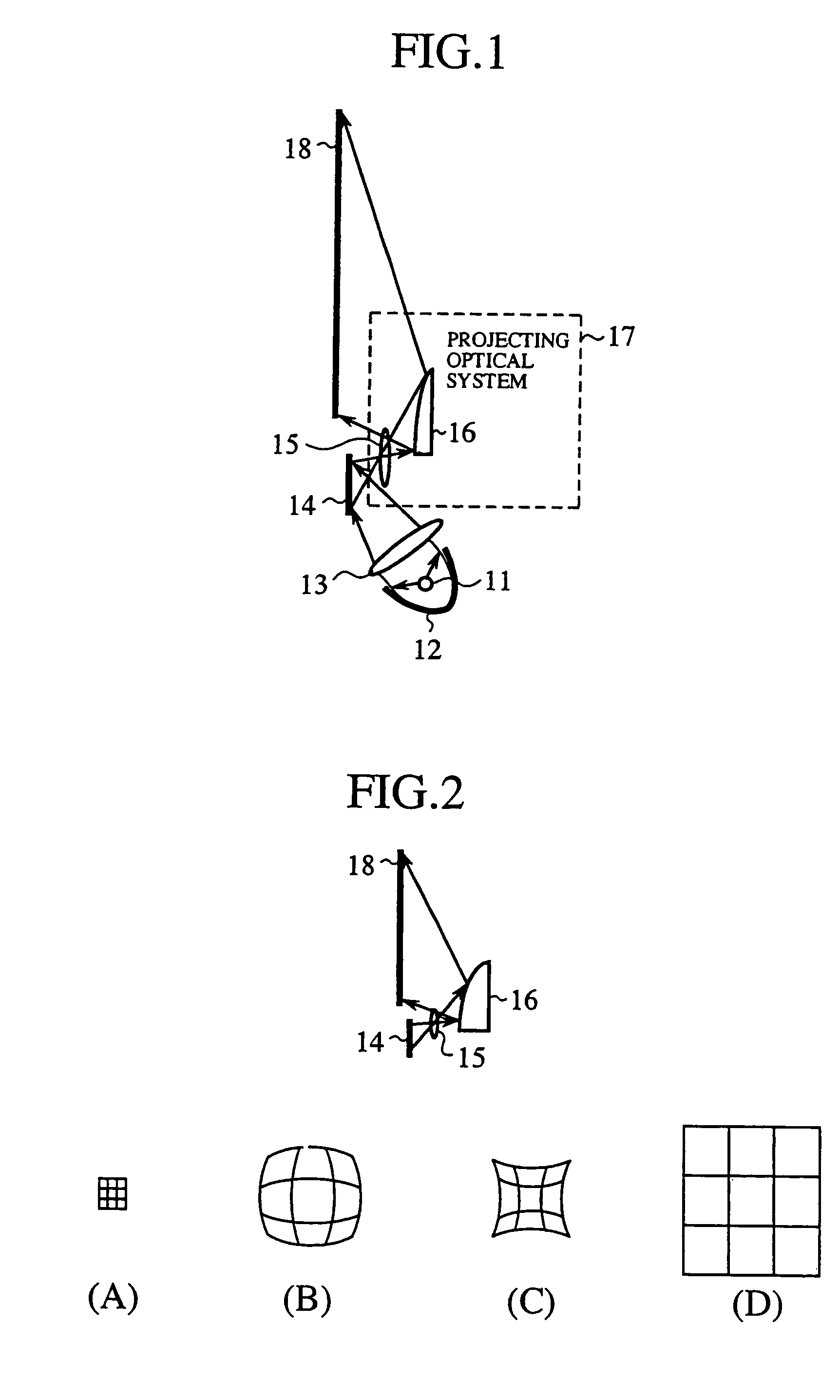
[0194]FIG. 1 schematically illustrates the configuration of an image display device according to a first embodiment (Embodiment 1) of the present invention. Reference numeral 11 denotes a luminous element that emits light (illumination light); 12 denotes a parabolic reflector for reflecting the light from the luminous element 11 mostly into parallel rays of light; and 13 denotes a condenser lens for gathering the rays of light reflected by the parabolic reflector 12. The luminous element 11, the parabolic reflector 12 and the condenser lens 13 constitute a illumination light source system (sending means, illumination light source part).

[0195]Reference numeral 14 denotes a micro-mirror device (sending means, a reflecting image information imparting part, digital micro-mirror device (DMD), a registered trademark of Texas Instruments Incorporated (TI)) that is a reflecting spatial light modulator. The micro-mirror device 14 spatially intensity-modulates the light gathered by the conden...

embodiment 2

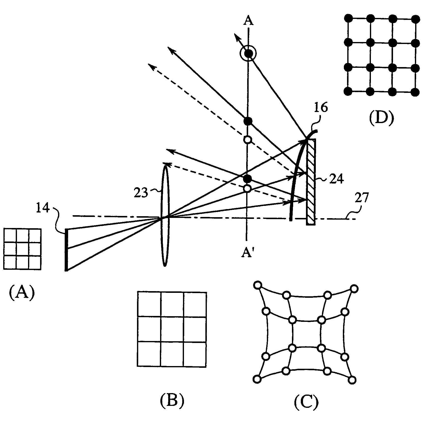
[0219]While in Embodiment 1 the projecting optical system 17 is comprised of the refracting optical lens 15 of barrel distortion and the convex mirror 16 of pincushion distortion, this embodiment (Embodiment 2) forms the projecting optical system by a Fresnel mirror capable of magnifying an image with a short projection distance as is the case with the convex mirror and having no distortion.

[0220]FIG. 5 is a diagram schematically depicting the configuration of an image display device according to Embodiment 2. Reference numeral 23 denotes an aplanatic refracting lens (a refracting optical part); 24 denotes a Fresnel mirror (a reflecting part) for reflecting light from the refracting optical lens 23 onto the screen 18; and 25 denotes a projecting optical system (projecting optical means) composed of the refracting optical lens 23 and the Fresnel mirror 24. As is the case with the convex mirror 16, the reflecting surface of the Fresnel mirror 24 has negative power. For brevity sake, n...

embodiment 3

[0225]In this embodiment the projecting optical system is made up of an optical element that has a convex projecting surface on the side thereof opposite the light receiving surface and a refracting optical lens.

[0226]FIG. 8 is a diagram schematically illustrating the configuration of an image display device according to a third embodiment (Embodiment 3) of the present invention. Reference numeral 28 denotes a refracting optical lens (a refracting optical part); 29 denotes an optical element (a reflecting part) formed of two optical materials of different dispersion characteristics; and 30 denotes a projecting optical system (projecting optical means) made up of the refracting optical lens 28 and the optical element 29. For the brevity sake, no illumination light source system is shown.

[0227]FIG. 9 depicts the optical element in enlarged dimension. Reference numerals 31 and 33 denote low dispersion glass (low dispersion medium) and high dispersion glass (high dispersion medium), res...


PUM


Abstract

An image display device includes an optical imaging arrangement for providing image information to illumination light and for transmitting the image information as an optical image signal; a projecting optical arrangement for receiving the optical image signal and for projecting the optical image signal; a display for receiving the optical image signal through the projecting optical arrangement and for displaying an image based on the image information; and a plane mirror for reflecting the optical image signal output from the projecting optical arrangement on the display.

Description

[0001]This application is a divisional of application Ser. No. 10 / 639,425, filed on Aug. 13, 2003, now U.S. Pat. No. 6,824,274 which is a divisional of application Ser. No. 09 / 852,031, filed on May 10, 2001 and issued as U.S. Pat. No. 6,631,994 on Oct. 14, 2003, the entire contents of which are hereby incorporated by reference and for which priority is claimed under 35 U.S.C. § 120; and this application claims priority of application Ser. Nos. 2000-137602 filed in Japan on May 10, 2000; 2000-241757 filed in Japan on Aug. 9, 2000; 2000-273723 filed in Japan on Sep. 8, 2000; 2000-313652 filed in Japan on Oct. 13, 2000; 2000-345571 filed in Japan on Nov. 13, 2000; and 2001-40739 filed in Japan on Feb. 16, 2001 under 35 U.S.C. § 119.BACKGROUND OF THE INVENTION[0002]1. Field of the Invention[0003]The present invention relates to an image display device by which an optical image signal based on image information is projected onto a display means to display an image, and a method for adjus...

Claims


Application Information

Patent Timeline
Patent Type & Authority Patents(United States)
IPC IPC(8): G03B21/22G03B21/28G02B7/02G02B3/08G02B5/09G02B7/09G02B7/18G02B7/28G02B7/36G02B13/16G02B13/18G02B17/08G02B27/00G02B27/18G03B21/00H04N5/74H04N9/12H04N17/00
CPCG02B5/09H04N9/3194G02B7/28G02B13/16G02B13/18G02B17/002G02B17/08G02B17/0852G02B17/086G02B27/0025G02B27/18G03B21/10G03B21/28H04N5/74H04N9/317G02B7/181H04N5/7458H04N9/12H04N9/3141H04N9/3147G03B21/16G03B21/53
Inventor SUZUKITERAMOTO, KOHEISUZUKI, JIROSHIKAMA, SHINSUKE
Owner MITSUBISHI ELECTRIC CORP
Why Eureka
Try Eureka