Supercharge Your Innovation With Domain-Expert AI Agents!

Memory cells with nonuniform floating gate structures

a floating gate, memory cell technology, applied in the direction of semiconductor devices, electrical devices, transistors, etc., can solve the problems of degrading the endurance of flash memory devices, affecting the generation of interface traps, and losing data stored in volatile memory devices

Inactive Publication Date: 2006-02-14
SAMSUNG ELECTRONICS CO LTD
View PDF2 Cites 2 Cited by
  • Summary
  • Abstract
  • Description
  • Claims
  • Application Information

AI Technical Summary

Benefits of technology

This configuration enables reduced program and erase voltages while enhancing the endurance of flash memory devices by concentrating the electric field and minimizing hole tunneling, thus improving the device's performance and reliability.

Problems solved by technology

Generally, a volatile memory device loses data stored therein when a power supply to the cell is removed.
The electrons may be caught in the interface traps when tunneling, such that the endurance of the flash memory device may be degraded.
Holes, having an effective mass larger than electrons, can seriously affect the generation of the interface trap.

Method used


Image

  • Memory cells with nonuniform floating gate structures
  • Memory cells with nonuniform floating gate structures
  • Memory cells with nonuniform floating gate structures

Examples


Embodiment Construction

[0029]The present invention will be described more fully hereinafter with reference to the accompanying drawings, in which preferred embodiments of the invention are shown. This invention, however, be embodied in many different forms and should not be construed as limited to the embodiments set forth herein. Rather, these embodiments are provided so that this disclosure will be thorough and complete, and will fully convey the scope of the invention to those skilled in the art. In the drawings, the thickness of layers and regions are exaggerated for clarity. It will also be understood that when a layer is referred to as being “on” another layer or substrate, it can be directly on the other layer or substrate, or intervening layers may also be present.

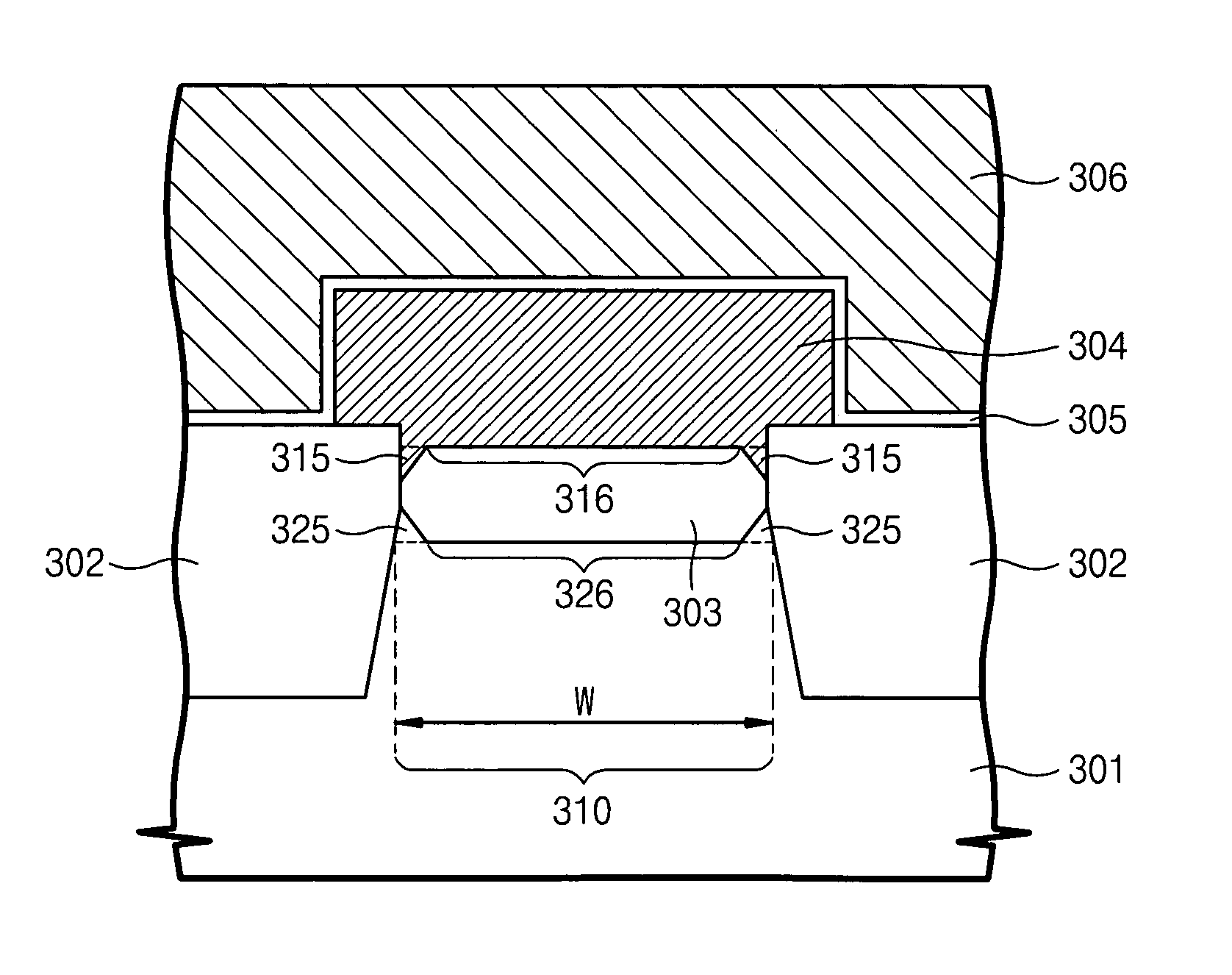
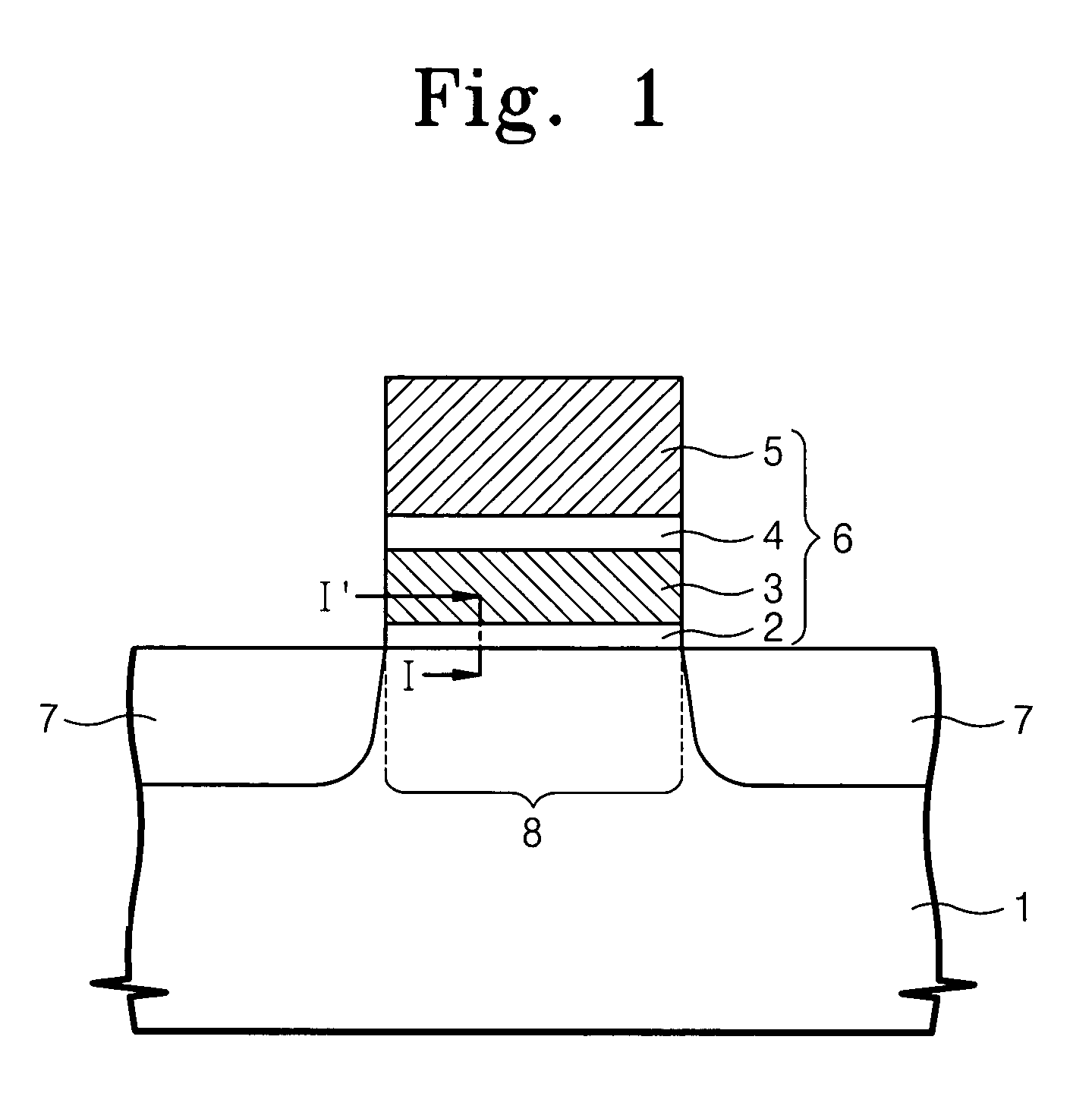
[0030]FIG. 3 is a top plane view of a nonvolatile memory cell according to an exemplary embodiment of the present invention. FIG. 4 is a cross-sectional view taken along a line II–II′ of FIG. 3.

[0031]Referring to FIGS. 3 and 4, a device ...


PUM


Abstract

In a floating gate memory cell including a floating gate separated from an active region by a tunnel isolation region, a first one of the active region and the floating gate comprises a portion that protrudes towards a second one of the active region and the floating gate. In some embodiments, the protruding portion tapers toward the second one of the active region and the floating gate. The tunnel insulation layer may be narrowed at the protruding portion. Protruding portions may be formed on both the floating gate and the active region.

Description

RELATED APPLICATION[0001]This application claims the benefit of Korean Patent Application No. 10-2002-0076956, filed on Dec. 5, 2002, which is incorporated herein in its entirety by reference.BACKGROUND OF THE INVENTION[0002]The present invention generally relates to memory devices and fabrication thereof, and more particularly, to floating gate nonvolatile memory cells and fabrication thereof.[0003]Semiconductor memory devices may be classified into volatile memory devices and non-volatile memory devices. Generally, a volatile memory device loses data stored therein when a power supply to the cell is removed. In contrast, a non-volatile memory device typically does not lose data (or loses data at a relatively slow rate) when power is removed. DRAM and SRAM devices are generally classified as volatile memory devices and flash memory devices are classified as nonvolatile memory devices.[0004]FIG. 1 is a cross-sectional view of a unit cell of a conventional flash memory device. FIG. 2...

Claims


Application Information

Patent Timeline
Patent Type & Authority Patents(United States)
IPC IPC(8): H01L29/788H01L21/8247H01L21/28H01L29/423
CPCH01L21/28273H01L29/7883H01L29/42336H01L29/42324H01L29/40114H10B99/00
Inventor LEE, JAE-DUKPARK, DONG-GUNCHOI, JEONG-HYUK
Owner SAMSUNG ELECTRONICS CO LTD
Features
  • R&D
  • Intellectual Property
  • Life Sciences
  • Materials
  • Tech Scout
  • Unparalleled Data Quality
  • Higher Quality Content
  • 60% Fewer Hallucinations
Learn More