Method of forming a micro solder ball for use in C4 bonding process

a technology of micro solder balls and c4 bonding, which is applied in the direction of electrical equipment, semiconductor devices, semiconductor/solid-state device details, etc., can solve the problems of increasing circuit complexity, increasing the number of input/output terminals of chips, and increasing the number of ic chip packages, etc., and achieves the effect of small conta

Inactive Publication Date: 2006-02-14
MICRON TECH INC
View PDF16 Cites 25 Cited by
  • Summary
  • Abstract
  • Description
  • Claims
  • Application Information

AI Technical Summary

Benefits of technology

[0015]The present invention provides an improved method for forming solder balls used in a C4 bonding process. The present inventor has discovered that by using a tape liftoff process to form the solder contacts, significantly smaller contacts can be easily formed on an IC chip.

Problems solved by technology

One of these involves increasing the circuit complexity of IC circuits which also often results in a larger package for the IC chip and an increase in the number of input / output (I / O) terminals for chip.
This method of connection was limited by the number of pads which could be placed on the periphery of the IC chip.
However, this technology is still limited by the number of pads which can be formed on the chip periphery, and therefore the number of I / Os on a chip is likewise limited.
Hence, the number of contacts that can be fabricated through use of a metal mask is limited because the holes in the mask must remain above a minimum size to prevent these problems.
Consequently, the size of the solder balls that can be created is similarly limited.

Method used


Image

  • Method of forming a micro solder ball for use in C4 bonding process
  • Method of forming a micro solder ball for use in C4 bonding process
  • Method of forming a micro solder ball for use in C4 bonding process

Examples


Embodiment Construction

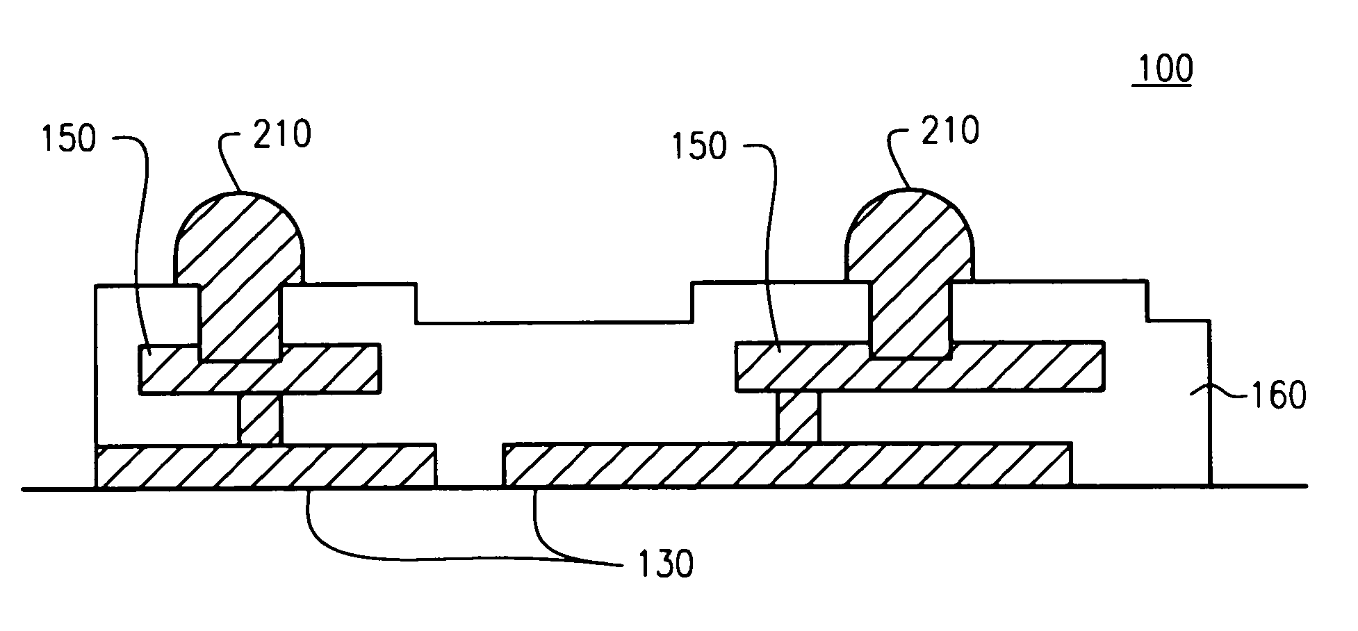
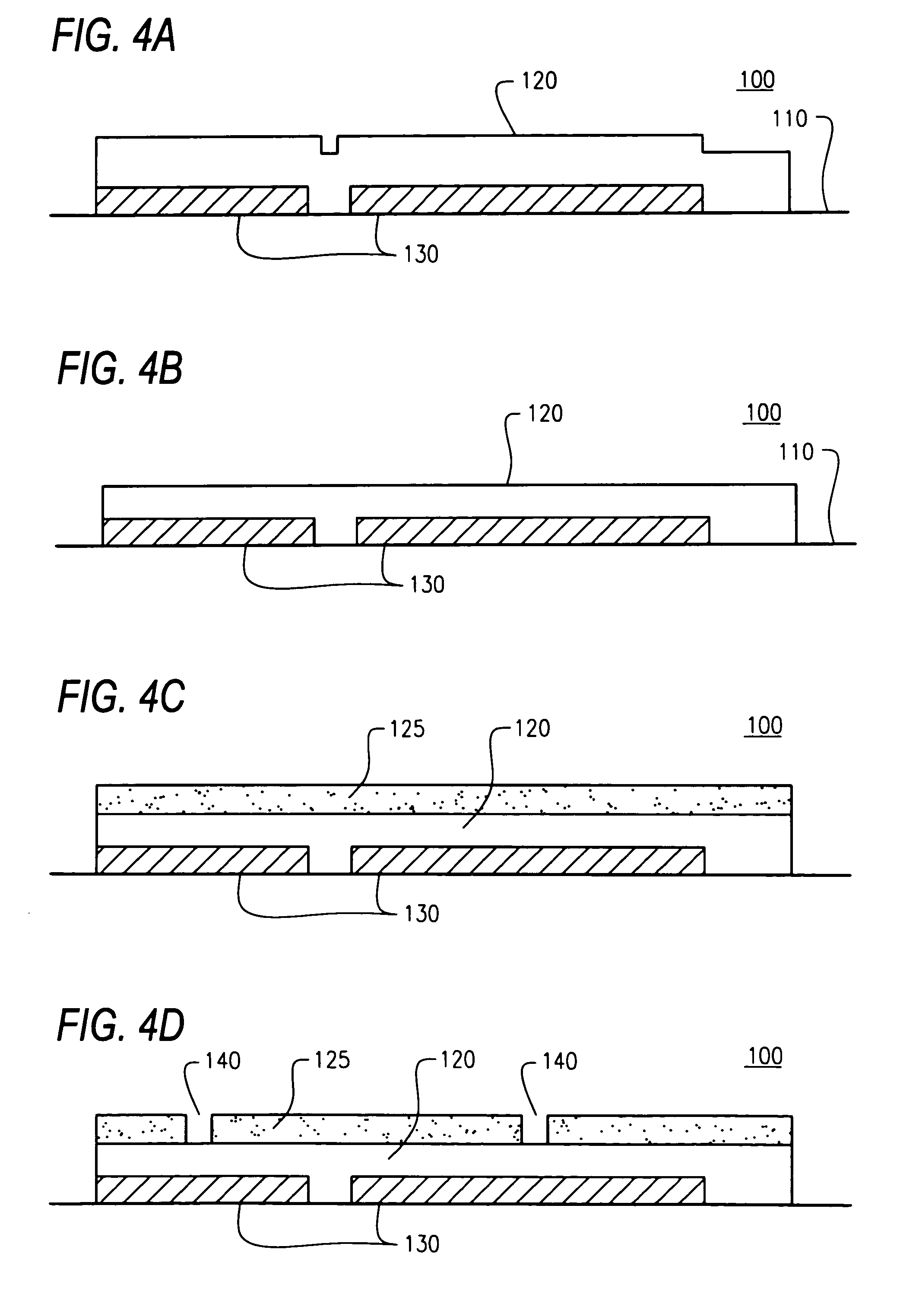
[0024]The present inventor has discovered that by using a tape liftoff process for screening solder balls onto a substrate, the size of the solder balls can be significantly decreased. The process described below can be used to deposit solder balls on an IC chip, a module substrate, a circuit board, or any similar substrate. Tape liftoff processes, per se, are known in the art, as evidenced by U.S. Pat. No. 5,240,878 to Fitzsimmons, which is incorporated herein by reference. Tape liftoff processes are frequently used to remove unwanted photoresist levels once an imaging and etching has taken place.

[0025]The process of the invention is explained below with reference to FIGS. 4A–4Q. Although the following explanation refers to a technique for placing solder balls on a wafer, those skilled in the art will recognize that the process described below can be performed on a single chip. Further, it will also be apparent to those skilled in the art that the process described below can be use...


PUM

PropertyMeasurementUnit
thicknessaaaaaaaaaa
diameteraaaaaaaaaa
diameteraaaaaaaaaa

Abstract

A method of forming micro solder balls for use in a C4 process is described. The solder balls are formed by laying down a peel-away photoresist layer, forming holes in the photoresist layer to expose electrical contacts, depositing a solder layer over the photoresist, forming solder areas in the holes and then, using a tape liftoff process to remove the solder layer and photoresist layer while leaving solder areas in the holes. The solder areas are then heated to allow solder balls to form.

Description

[0001]This application is a divisional of application Ser. No. 09 / 134,363, filed on Aug. 14, 1998, now U.S. Pat. No. 6,136,689, which is hereby incorporated by reference.BACKGROUND OF THE INVENTION[0002]1. Field of the Invention[0003]The invention relates to a method of forming micro solder balls for bonding integrated circuits to a module substrate or to a circuit board, using a C4 bonding process. In particular, there is described a method for forming micro solder balls by a tape liftoff process which allows for an increased number and density of input / ouput connections to be fabricated on each integrated circuit chip, module substrate or circuit board.[0004]2. Description of the Related Art[0005]The central processing units (CPUs) of most modern day computers are typically provided on large circuit boards (mother boards) populated with various integrated circuit (IC) chips, such as microprocessor chips and memory chips. These IC chips work in conjunction with one another to perfo...

Claims


Application Information

Patent Timeline
Patent Type & Authority Patents(United States)
IPC IPC(8): H01L23/48H01L23/52H01L29/40H01L21/48H01L21/60H01L23/485
CPCH01L21/4853H01L24/11H01L24/13H01L2924/0001H01L2224/131H01L2924/014H01L2224/13099H01L2224/16225H01L2924/01009H01L2924/01013H01L2924/01029H01L2924/0104H01L2924/01079H01L2924/14H01L2924/01005H01L2924/01006H01L2924/01033H01L2924/01076
Inventor FARRAR, PAUL A.
Owner MICRON TECH INC
Why Eureka
Try Eureka